
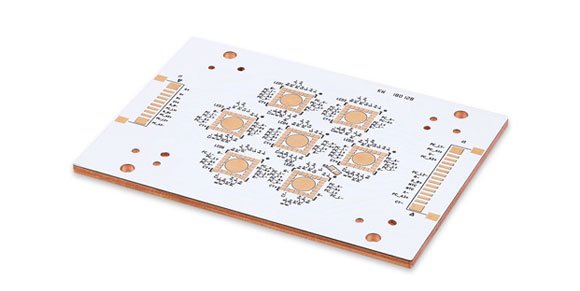
Designing PCBs? That copper layer hides surprises. Forget guesses or costly mistakes.
1 oz copper[^1] is precisely 1.37 mils (0.00137 inches) or 35 µm thick. This standard forms when 1 ounce of copper spreads evenly over 1 square foot of board. It balances cost and conductivity for everyday electronics.

Wondering how this copper weight affects your design? I’ve seen boards fail from simple copper choices. Stick around as we explore practical thickness rules.
What is the standard thickness of copper?
Thin copper causes broken traces. Too thick wastes money. What’s the sweet spot?
1 oz copper (1.37 mils/35 µm) is the universal default. It handles 1-3A per trace millimeter. Lighter 0.5 oz suits low-power devices. Heavier 2-3 oz options serve power systems and high-heat areas.

Matching copper weight to real needs
Choosing copper isn’t about extremes. Cost spikes with thicker layers, and etching gets tricky. For general digital boards below 100MHz? Stick with 1 oz. I once overdesigned a Bluetooth module with 2 oz copper – manufacturing costs doubled for zero benefit.
Critical factors shaping copper choice:
| Application | Recommended Copper | Why? |
|---|---|---|
| Consumer electronics | 0.5 – 1 oz | Cost efficiency, adequate conductivity |
| Power supplies | 2 – 3 oz | Handles high currents, reduces heating |
| RF/microwave circuits | 0.5 oz | Precision etching for fine traces |
| Automotive/Aerospace | 2 oz minimum | Extreme temperature stability & vibration resistance |
| Prototypes | 1 oz | Balances cost, availability, and testing flexibility |
Notice environmental stress[^2]? Aircraft boards need rugged copper. But that weather station on your porch? Standard 1 oz does fine. Thicker copper also increases board weight – critical for satellites.
How does PCB copper thickness impact manufacturing?
Ignoring copper specs risks production disasters. Why does 1 oz dominate factories?
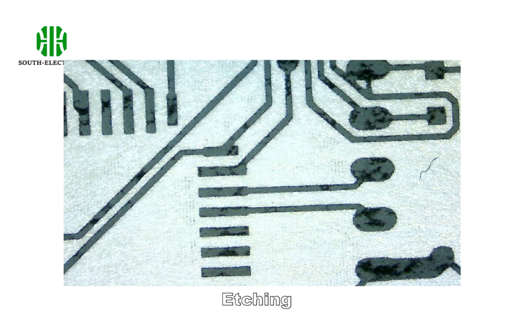
Thicker copper complicates etching and raises costs. Each 1 oz increase demands 30% more etch time and tighter process control. Standard 1 oz works with any fab house. Deviations cause delays and yield drops.
The manufacturing ripple effect
Copper thickness impacts every fabrication step. Imagine etching 3 oz copper – it’s like carving stone versus slicing paper. Chemical baths require recalibration. I recall a client insisting on 4 oz for "durability" – their prototype costs tripled.
Here’s how thickness shifts production:
| Thickness | Etching Time | Tolerance | Cost Multiplier | Yield Impact |
|---|---|---|---|---|
| 0.5 oz | Standard | ±0.2 mm | 0.9x | Minimal |
| 1 oz (Standard) | Baseline | ±0.3 mm | 1.0x | Optimal |
| 2 oz | +40% | ±0.5 mm | 1.8x | Moderate |
| 3 oz+ | +70-100% | ±0.8 mm | 3.0x+ | Significant |
Thinner copper enables finer traces – 0.5 oz achieves 3mil lines versus 1 oz’s 5mil minimum. But electrical engineers often crave thicker copper’s current capacity[^3]. It’s a tangible trade-off.
When to use 2oz copper PCB?
Thin copper melts under stress. When is heavier better?
Switch to 2 oz copper (2.74 mils/70 µm) anywhere trace currents exceed 3A. This prevents overheating in power supplies[^4], motor controllers, and LED arrays. The doubled thickness handles heat and vibrations far better.

Spotting the 2 oz application sweet spots
Don’t overapply heavy copper. It transforms boards like muscle fibers bulk up. In server power units I design? 2 oz handles 100A surges. Your smartwatch charger? Stick to 1 oz.
Clear signals demanding 2 oz:
- Thermal hotspots: Heat-sinking components need thick copper planes
- Connector points: Repeated plugging strains thin copper traces
- High-amplitude signals: Power MOSFETs/RF transmitters require stable planes
- Wide traces: Anything thicker than 12mm benefits from weight support
- Harsh environments: -40℃ to 150℃ cycling fatigues thin copper
Calculate your necessity: A 1 oz 20mm trace handles 8.5A max before heat spikes. Upgrade that to 2 oz, it manages 15A. That drone’s ESC? Exactly why I specify 2 oz – sudden motor surges cook thinner boards.
When isn’t increased PCB copper thickness always the answer?
Heavier feels safer. But why do seasoned designers resist stacking copper?
Thick copper disrupts impedance control[^5] and signal integrity[^6]. High-frequency traces over 100MHz become unstable on 2 oz+ boards. Every ounce added raises manufacturing costs by 25-40% and limits trace precision.

I learned this debugging a 5GHz Wi-Fi module. 2 oz copper caused impedance drift – a nightmare for milliwatt signals. Beyond cost, physics works against you.
Key limitations:
| Problem Area | 1 oz Copper | 2 oz Copper | Why It Matters |
|---|---|---|---|
| Minimum Trace Width | 5 mil (0.13 mm) | 8 mil (0.20 mm) | Blocks dense circuitry |
| Etching Tolerance | ±15% | ±25% | Creates impedance mismatches |
| Signal Loss (10 GHz) | 1 dB/cm | 1.8 dB/cm | Kills high-frequency performance |
| Material Cost | $ | $$$ | Directly hits production budgets |
| Drill Breakage | Rare | Common > 0.3 mm holes | Increases board defects |
The signal loss difference shocked me. At 24 GHz radar frequencies? 1 oz gives you usable signals; 2 oz drops data rates drastically. Also, remember: thicker copper means thicker prepreg layers during lamination – a forgotten factor affecting dielectric constants.
Conclusion
PCB copper thickness balances electrical needs against physical realities. Standard 1 oz (35µm) suffices for 80% of designs. Use 2 oz only where heat or current demands it – high frequencies demand lean copper.
[^1]: Understanding the role of 1 oz copper can help you optimize your PCB designs for cost and performance.
[^2]: Understanding environmental stress can help you make informed decisions about copper thickness in your designs.
[^3]: Explore how copper thickness directly influences the current capacity of your PCB designs.
[^4]: Learn about the specific copper needs for power supplies to ensure efficient performance.
[^5]: Explore the critical role of impedance control in ensuring signal integrity in your designs.
[^6]: Learn about the various factors that can impact signal integrity and how to mitigate issues.

