
Is it possible to 3D print a PCB?
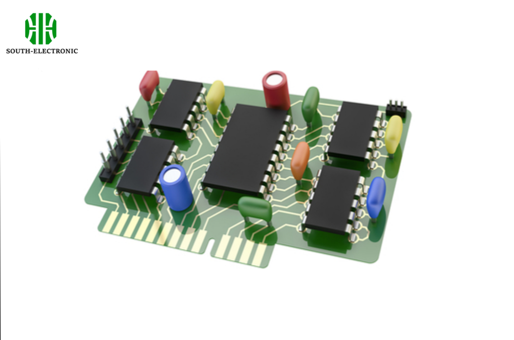
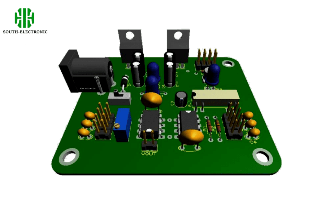
Yes, 3D printing PCBs is a viable and innovative method for creating circuit boards. The process involves layering conductive and non-conductive materials to build the PCB structure. 3D printing PCBs can revolutionize PCB design by enabling faster, cheaper, and more innovative production.
How does PCB printing work?
PCB printing begins after designers output the PCB schematic files and manufacturers conduct a DFM check. Manufacturers use a special printer called a plotter, which makes photo films of the PCBs, to print circuit boards.
Step-by-Step Process
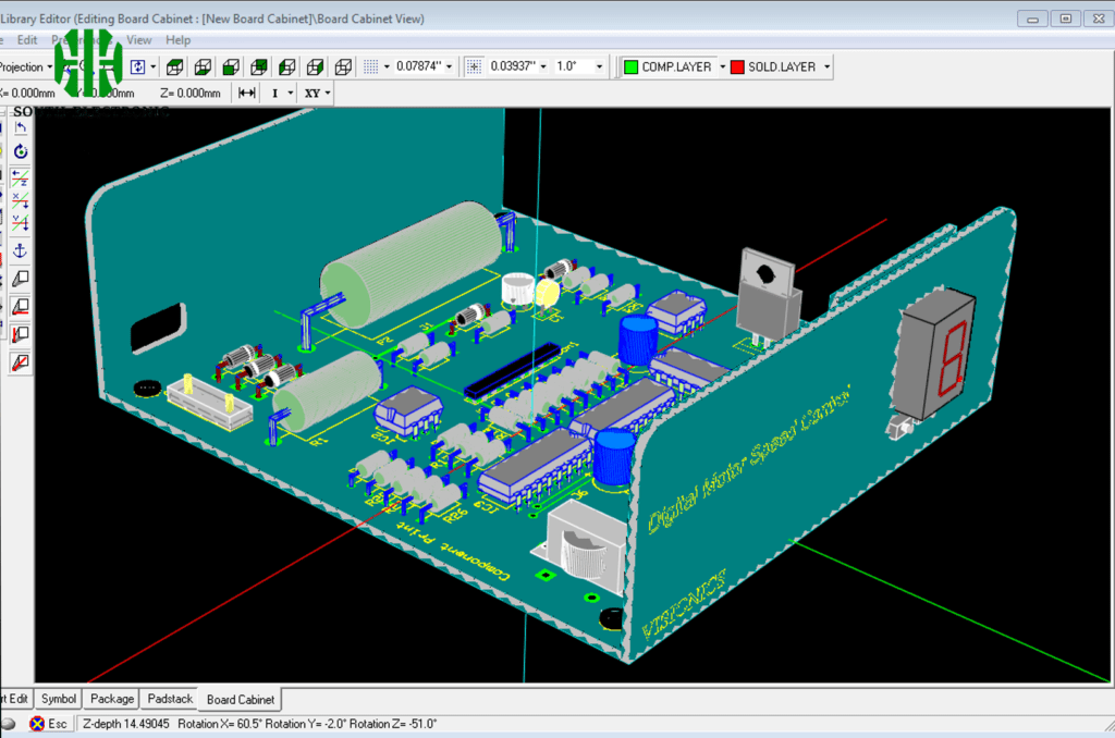
- Design the PCB Schematic: Use software like Eagle or KiCad to create the PCB layout.
- Prepare the 3D Printer: Load the printer with conductive and non-conductive filaments.
- Print the PCB: Layer by layer, the printer builds the PCB according to the design.
- Post-Processing: Clean the PCB and inspect for any defects.
How to print PCB?
Printing PCBs at home is feasible with the right tools and materials. Here’s a detailed guide:
Materials Required
- Copper Clad Board: Base material for the PCB.
- Ferric Chloride: For etching the copper.
- Laser Printer: For printing the PCB layout.
- Iron: For transferring the layout to the copper board.
Step-by-Step Instructions
| Step | Description |
|---|---|
| Layout Design | Use software to create the PCB layout. |
| Printing | Print the layout on glossy paper using a laser printer. |
| Transferring | Iron the layout onto the copper board. |
| Etching | Submerge the board in ferric chloride. |
| Drilling | Drill holes for components. |
Tips for Success
- Ensure Proper Heat Transfer: Use a hot iron and apply even pressure.
- Use Fresh Ferric Chloride: For effective etching.
- Clean the Board: Thoroughly clean the copper board before starting.
What troubleshooting tips should I know for 3D printing PCBs?
- Print Quality Issues: Ensure the printer is calibrated correctly and the filaments are of high quality.
- Material Compatibility: Use materials compatible with your printer and design.
- Design Errors: Double-check the schematic and layout for errors before printing.
- Regular Maintenance: Keep your printer well-maintained and clean.
- Test Prints: Conduct test prints to ensure quality and accuracy.
- Consult Forums: Engage with online communities for advice and troubleshooting.
How does 3D printing PCBs differ from traditional PCB manufacturing?
| Factor | Traditional Manufacturing | 3D Printing |
|---|---|---|
| Cost | High | Low |
| Lead Time | Long | Short |
| Flexibility | Limited | High |
| Equipment Required | Expensive | Affordable |
| Material Options | Limited | Diverse |
Traditional PCB manufacturing can be time-consuming and costly, especially for prototyping and small-scale production. 3D printing PCBs offers a faster, cheaper, and more innovative solution for PCB design, potentially resolving the electronics industry’s supply issues.

