

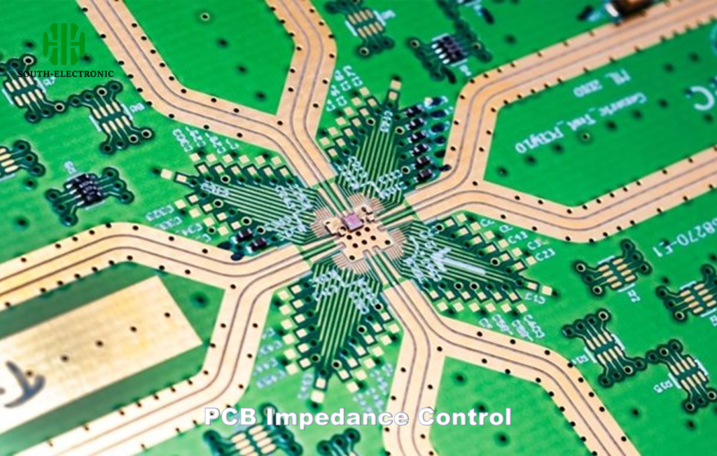
Signal distortion ruining your high-speed PCB designs? Uncontrolled impedance causes reflections, data errors, and system failures. Modern electronics demand precise impedance control to prevent these costly issues. Let’s explore how to achieve target impedance for reliable performance.
To achieve target PCB impedance control, designers adjust trace geometry (width/height), dielectric material selection, and layer spacing using specialized calculators and simulation tools. This ensures consistent electrical characteristics across high-speed signal paths.
Mastering impedance control starts with understanding five foundational concepts. We’ll break down each element through real design scenarios and practical adjustment techniques.
What Is Controlled Impedance in PCB?
Ever wonder why identical-looking traces behave differently electrically? Controlled impedance maintains consistent resistance to alternating current throughout a trace’s length. It’s the hidden factor determining signal quality in modern PCBs.
Controlled impedance in PCB refers to maintaining specific resistance (Z) to AC signals through precise trace dimensions and material selection. It ensures signals transmit without distortion in high-frequency applications (1MHz+).
Key Impedance Components
| Factor | Typical Range | Impact on Z | Control Method |
|---|---|---|---|
| Trace width | 4-12 mil | Narrower = Higher Z | Etching tolerance control |
| Dielectric constant (Dk) | 3.5-4.5 | Lower Dk = Higher Z | Material selection |
| Copper thickness | 0.5-2 oz | Thinner = Higher Z | Plating process control |
| Trace height | 3-5 mil | Taller = Lower Z | Prepreg selection |
| Spacing to plane | 5-15 mil | Closer = Lower Z | Layer stacking |
Example: A 50Ω microstrip line with FR-4 material (Dk=4.2) requires 8 mil width when using 1.6mm substrate thickness. Change to Rogers 4350B (Dk=3.48), and the width drops to 6.5 mil for same impedance.
Why Is Impedance Control Critical for High-Speed PCBs?
Lost 40% of your signal strength before reaching the IC? Impedance mismatches cause power loss and data corruption that escalates with frequency. DDR5 interfaces require <5% impedance tolerance across entire bus routes.
Impedance control prevents signal reflections and power loss in high-speed designs. Proper matching ensures complete signal transfer between components with frequencies above 100MHz.

High-Speed Failure Modes
| Issue | Cause | Effect | Solution |
|---|---|---|---|
| Signal reflection | Z mismatch at junctions | Data errors | Use termination resistors |
| EMI radiation | Impedance discontinuities | Failed FCC tests | Maintain constant Z path |
| Timing jitter | Phase distortion | Clock sync failures | Match intra-pair Z within 2% |
| Power loss | Impedance variation | Reduced SNR | Optimize Dk consistency |
PCIe 5.0 designs require ±8% impedance control (56Ω±4.48Ω). A 10% deviation causes 3dB loss in signal integrity – equivalent to 50% power loss per interface.
Which Design Parameters Most Affect Target Impedance?
Why do identical trace widths yield different impedances? Six key parameters interact to determine final impedance values. Controlling these variables separates successful designs from failed prototypes.
Trace width (35% impact), dielectric thickness (30%), copper thickness (15%), and material Dk (20%) most affect target impedance. Use controlled impedance calculators that account for all variables simultaneously.
Parameter Adjustment Guide
| Parameter | 10% Change Effect | Adjustment Method | Tolerance Control |
|---|---|---|---|
| Trace width | ±6Ω | Etching compensation | ±0.2 mil |
| Dielectric height | ±4Ω | Press-fit controls | ±2% thickness |
| Copper weight | ±1.5Ω | Plating monitoring | ±0.1 oz |
| Solder mask | ±0.8Ω | Coverage percentage | 85-95% cover |
| Plane spacing | ±3Ω | Layer alignment | ±1 mil shift |
Practical Example: Achieving 100Ω differential pair:
- Trace width: 5 mil
- Spacing: 5 mil
- Dielectric: Isola 370HR (Dk=4.0)
- Thickness: 3.5 mil
Resultant Z: 100.3Ω±1.2Ω using standard fab tolerances.
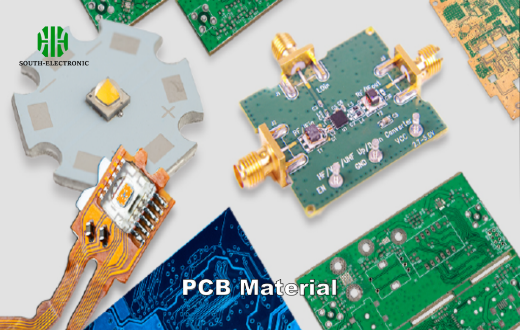
How Does Material Selection Impact Your Impedance Goals?
Frustrated by unpredictable Dk values? Material properties fundamentally determine achievable impedance ranges. FR-4’s ±10% Dk variation creates ±7Ω impedance shifts – catastrophic for 10Gbps+ designs.
PCB material selection impacts impedance through dielectric constant (Dk) stability and loss tangent. High-frequency materials like Rogers 4350B maintain ±2% Dk vs FR-4’s ±10%, enabling precise impedance control.
Material Performance Comparison
| Material | Dk @10GHz | Dk Tolerance | Cost Factor | Best Use Case |
|---|---|---|---|---|
| FR-4 | 4.2 | ±10% | 1x | <2GHz consumer |
| Rogers 4350B | 3.48 | ±2% | 5x | 5-40GHz RF |
| Isola FR408 | 3.7 | ±5% | 2x | 2-10GHz comms |
| Polyimide | 3.5 | ±8% | 3x | Flexible circuits |
| Nelco 4000-13 | 3.8 | ±3% | 4x | Mil/aero apps |
Case Study: Switching from FR-4 to Rogers 4350B reduced impedance variation from ±7Ω to ±1.5Ω in a 25Gbps SerDes design, enabling error-free operation at 32Gbaud.
Conclusion
Precise PCB impedance control requires coordinated adjustments to trace geometry, material selection, and manufacturing tolerances. Implement impedance calculators early, verify with field solvers, and prioritize Dk-stable materials for high-speed success.

