
Picking wrong copper thickness ruins boards. Your device overheats or fails. Avoid wasted prototypes by understanding key factors upfront. Save time and money now.
Select PCB copper thickness by evaluating current load, impedance needs, thermal demands, and cost. Thicker copper handles high currents but complicates impedance control. Thinner layers reduce cost and suit high-frequency signals.
Copper choice decides your PCB’s fate. Let’s break down the three critical questions every designer faces. This guides your decision step by step.
Choosing PCB Copper Thickness: When Thin, Thick or Mixed Makes Sense?
Ever fried a trace? Wrong copper thickness causes overheating. Choose smartly for reliability and performance. Avoid instant failures.
Thin copper (≤1 oz) suits signal integrity-focused designs. Thick copper (≥3 oz) powers high-current boards. Mixed layers optimize cost-performance balance for complex projects.

Matching Copper Weight to Design Needs
Consider these core requirements:
| Application | Recommended Copper | Key Advantage |
|---|---|---|
| High-frequency signals | 0.5-1 oz | Lower inductance |
| Power supplies | 2-6 oz | Current capacity |
| Cost-sensitive | 1-2 oz | Manufacturing savings |
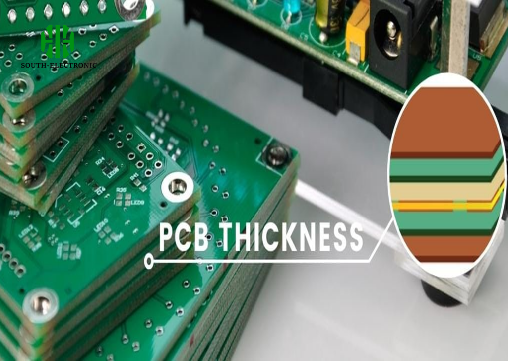
Trace width impacts current handling. Double copper thickness quadruples current capacity. Thermal relief matters too. Thicker copper clad pcb material spreads heat away from components.
Mixed stack-ups save money. Place thick copper only in power layers. Use standard 1oz copper for signal layers. This copper clad pcb board approach maintains impedance control while handling high current. Hybrid designs leverage heavy copper pcb benefits selectively.
For LED controllers, I combine 2oz inner layers with 1oz outer copper. This balances cost and heat dissipation in copper core pcb designs.
How Much Current Can Your PCB Copper Trace Handle?
Trace smoking under load? Undersized copper causes meltdowns. Prevent fire hazards through precise calculation. Know your limits.
Use IPC-2152 charts or online calculators. A 10mm-wide 2oz trace handles ~15A at 20°C rise. Thicker copper pcb dramatically boosts capacity without widening traces.
Calculating Safe Current Limits
Key parameters define your trace’s capacity:
| Factor | Effect on Current Rating |
|---|---|
| Copper thickness ↑ | Increases capacity |
| Trace width ↑ | Increases capacity |
| Ambient temperature ↑ | Decreases capacity |
| Surrounding copper | Improves heat dissipation |
Thick copper pcb traces require spacing adjustments. Heavy copper needs wider clearances between traces. Airflow impacts cooling too. Enclosed devices need derating by 15-20%.
Copper thickness on pcb impacts voltage drop. For power distribution, 3oz copper reduces drop by 30% versus 1oz. Thick copper pcb prevents brownouts in high-current zones. Test prototypes with 20% margin above maximum expected load. Exposed copper on pcb surfaces aids cooling but requires solder mask dams.
In motor drivers, I specify 4oz copper for 25A+ paths. This avoids pcb exposed copper failures during startup surges.
PCB Copper Thickness: How It Impacts Impedance Control & Signal Integrity
Signal distortions ruining data? Copper thickness shifts impedance. Maintain clean signals in high-speed designs. Beat signal loss.
Thinner copper improves high-frequency performance. 1oz copper reduces inductance versus thicker alternatives. Impedance tolerances tighten below ±5Ω with controlled copper pcb processes.

Balancing Thickness and Signal Performance
Signal integrity depends on three copper factors:
| Parameter | Thin Copper (0.5-1oz) | Thick Copper (≥2oz) |
|---|---|---|
| Skin effect loss | Lower | Higher |
| Impedance precision | Easier to control | Challenging |
| Crosstalk risk | Reduced with thin traces | Increases with width |
RF designs demand ≤1oz copper. Thicker layers increase capacitance between adjacent traces. Microwave boards often use 0.5oz copper pcb for minimal loss. Heavy copper pcb materials suit power planes only.
Differential pairs need exact impedances. The pcb board copper thickness variance must stay under ±10%. Production testing ensures specified ohms. Copper inlay pcb market growth addresses hybrid needs. For 5G routers, I use 0.8oz finished copper weight. This maintains 50Ω impedance across GHz frequencies.
Conclusion
Choose copper thickness after analyzing current, impedance, thermal and cost factors. Match thickness to each layer’s function. Balance performance with practicality always.

