
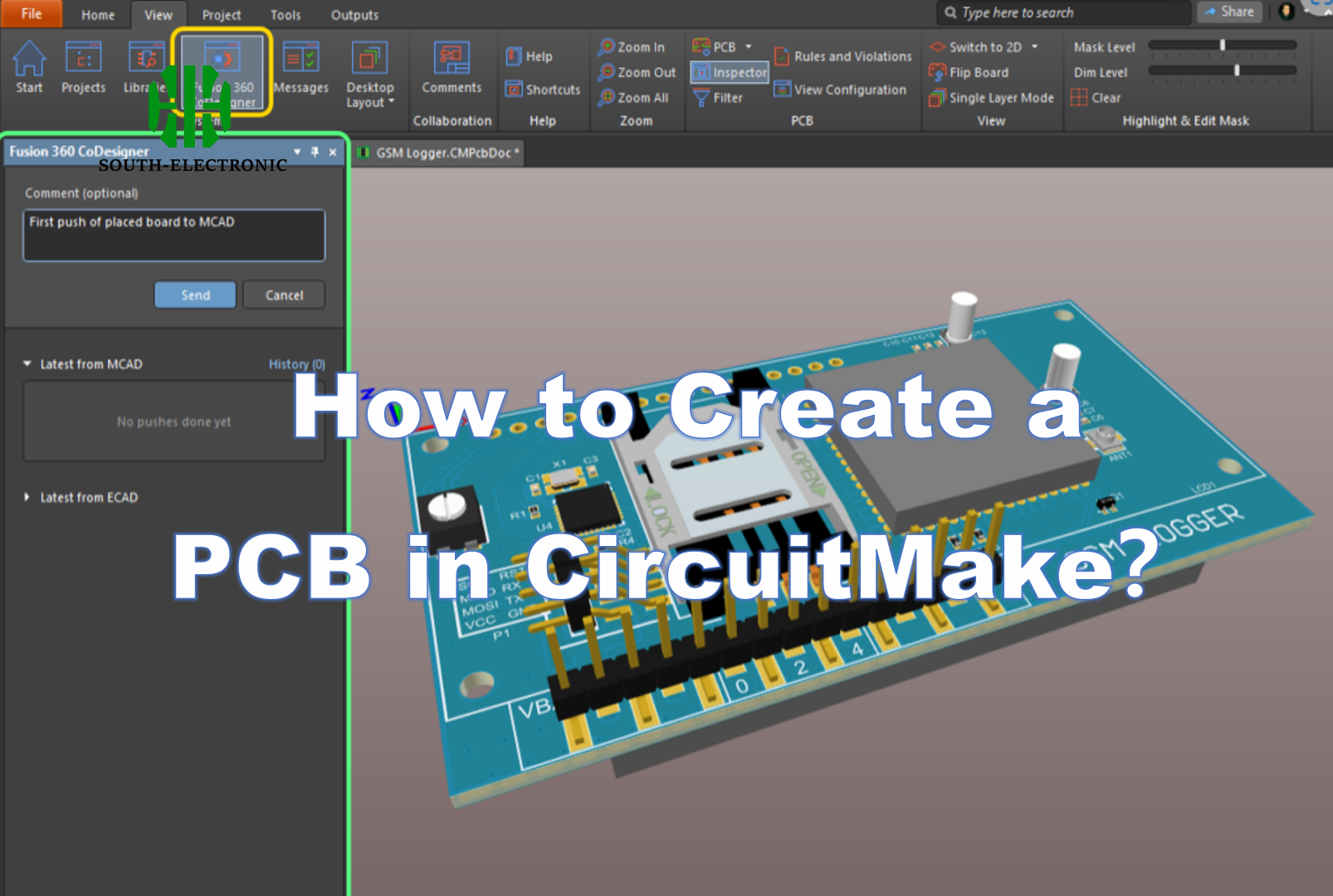
How to Create a PCB in CircuitMake?
To create a PCB in CircuitMaker, start by designing your schematic in the software. Once your schematic is complete, add a PCB footprint and adjust the board size. Next, lay out the components, route the traces, and fill copper. Finally, perform design rule checks (DRC) to ensure your board meets all specifications before exporting your design for manufacturing.
CircuitMaker simplifies this process with its user-friendly interface and powerful features. In this guide, I’ll walk you through each step of creating a PCB in CircuitMaker, from schematic design to final layout. Now that you understand the basic steps, let’s dive deeper into each stage of the PCB creation process in CircuitMaker.
1. How to Make a PCB Board Step by Step?
Creating a PCB involves several steps that must be followed meticulously to ensure the final design is functional and ready for manufacturing. Here’s a step-by-step guide on how to make a PCB in CircuitMaker.
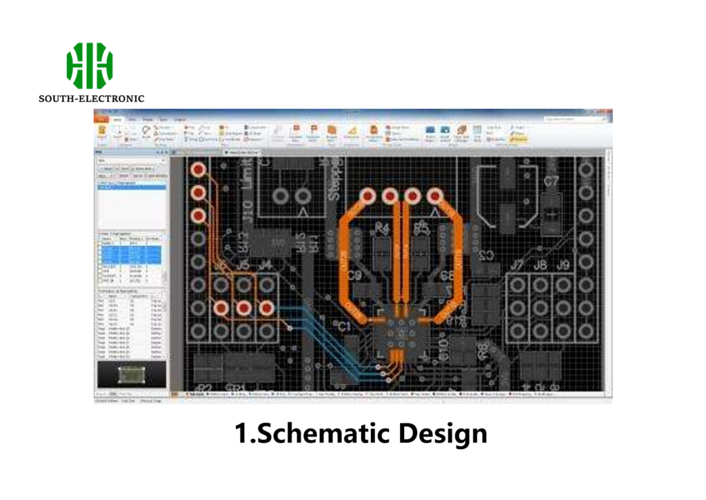
1.Schematic Design
The first step in PCB creation is designing the schematic. This is where you define the electrical connections between components.
- Create a New Project: Open CircuitMaker and select
File > New Project. Name your project and choose the folder where it will be saved. - Add Components: Use the component libraries to add all the necessary parts to your schematic. Place them on the canvas and connect them using wires.
- Annotate the Schematic: Ensure that all components are properly labeled with reference designators.
- Run Electrical Rule Check (ERC): This will help identify any potential issues in the schematic.
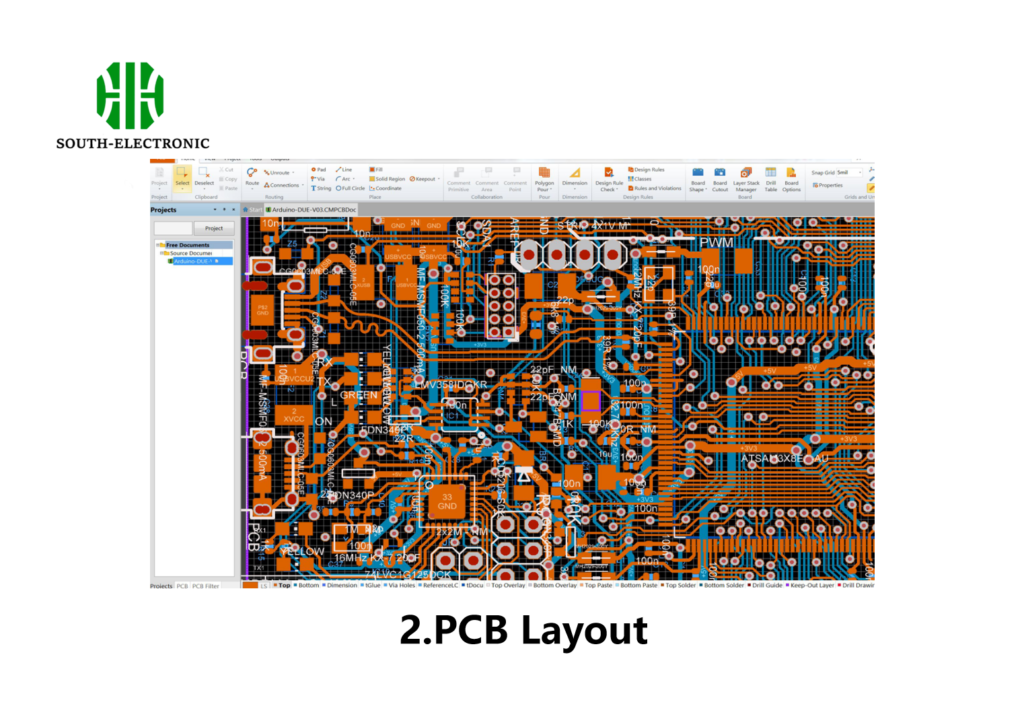
2.PCB Layout
Once your schematic is complete, it’s time to move on to the PCB layout. This is where you arrange the physical layout of the components on the board.
- Generate PCB Footprint: From the schematic, generate a PCB footprint by selecting
Project > Add New PCB. This will create a blank PCB layout. - Adjust Board Shape and Size: Modify the board outline to match the desired dimensions.
- Place Components: Use the
Component Placementtool to arrange components on the board as per your design requirements. - Route the Traces: Connect the components by routing the traces between them. Ensure that you follow the design rules for trace width and spacing.
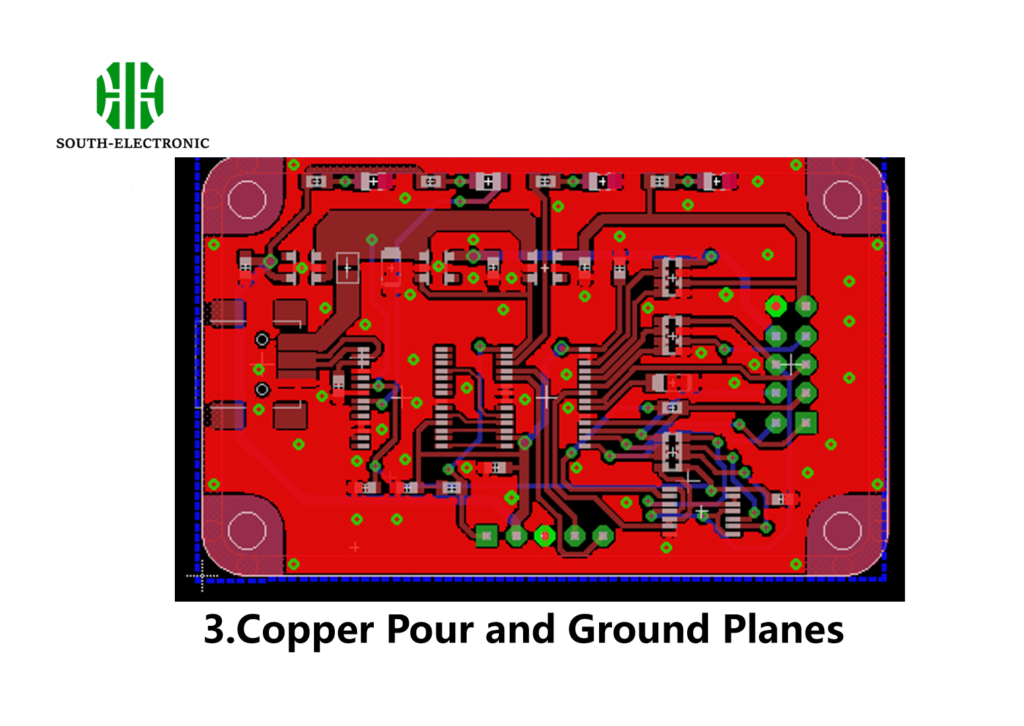
3.Copper Pour and Ground Planes
Copper pours are used to create ground planes and reduce noise in the circuit.
- Add Copper Pour: Select
Home > Copper Pourand choose the layer where you want to add the copper pour (e.g., the top or bottom layer). - Connect to Ground: Ensure that the copper pour is connected to the ground net in your circuit.
- Adjust Parameters: Modify the pour’s clearance, width, and other properties as needed.
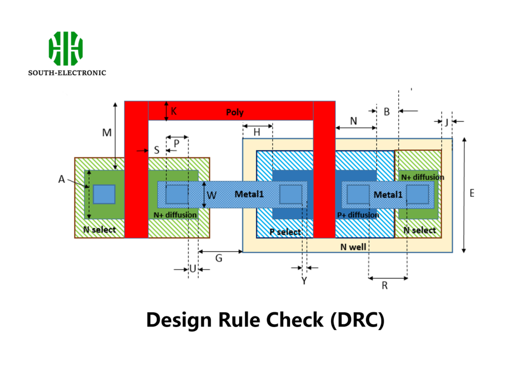
4. Design Rule Check (DRC)
Before finalizing your PCB, it’s essential to run a Design Rule Check (DRC) to identify any violations that might cause manufacturing issues.
- Run DRC: In CircuitMaker, select
Home > Design Rule Check. The software will check for clearance issues, unconnected nets, and other potential problems. - Review and Fix Issues: If any errors are found, review them and make the necessary adjustments.
Common DRC Errors and Solutions
| DRC Error | Description | Solution |
|---|---|---|
| Unrouted Net | A connection in the schematic has not been routed on the PCB. | Use the Routing tool to connect all nets. |
| Clearance Violation | Traces or components are too close to each other. | Increase the spacing between traces/components. |
| Short Circuit | Two nets that should not be connected are shorted together. | Identify the shorted nets and adjust routing or copper pour. |
| Overlapping Components | Components are placed too close, causing overlaps. | Reposition components to ensure they do not overlap. |
| Invalid Footprint | The footprint of a component does not match its schematic. | Update the footprint to match the component’s design in the schematic. |
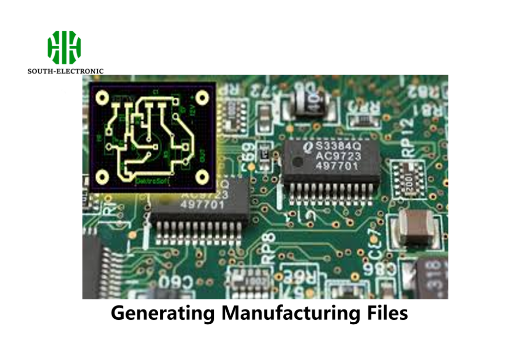
5. Generating Manufacturing Files
After completing the PCB design and ensuring there are no DRC errors, the next step is to generate the files needed for manufacturing.
- Generate Gerber Files: Go to
File > Fabrication Outputs > Gerber Files. These files are used by manufacturers to create the PCB. - Create Drill Files: Generate the drill files, which specify where holes need to be drilled on the PCB.
- Export Bill of Materials (BOM): The BOM lists all the components used in the design along with their specifications.
What are the Three Basic Methods to Make PCB?
There are several methods for creating PCBs, each with its own advantages and disadvantages.
1. Iron-on Glossy Paper Method
This method is commonly used for small-scale or hobbyist projects.
- Print the PCB Layout: Print the PCB layout onto glossy paper using a laser printer.
- Transfer the Layout to the PCB: Use an iron to transfer the toner from the paper to the copper board.
- Etch the Board: Use a ferr
ic chloride solution to etch away the unprotected copper, leaving only the traces.
2. Circuit by Hand on PCB
For simple designs, it’s possible to draw the circuit directly onto the PCB using a permanent marker.
- Draw the Circuit: Use a permanent marker to draw the circuit directly onto the copper board.
- Etch the Board: Etch the board as described in the previous method.
3. Laser Cutting and Etching
For more precise designs, a laser cutter can be used to create the PCB.
- Laser Cut the Layout: Use a laser cutter to remove unwanted copper from the board.
- Inspect the Board: Ensure that all traces are correctly cut and there are no shorts.

Creating a PCB in CircuitMaker is straightforward when you follow the right steps. From schematic design to final checks, this guide covers everything you need to know. Start your project today and take advantage of CircuitMaker’s robust tools to bring your electronic designs to life.

