
How to Deal with Crossing Wires?
When you’re designing a PCB, it’s inevitable that you’ll have to deal with crossing wires. It’s just a fact of life. But don’t worry, it’s not as complicated as it seems. In this article, I’ll show you a few different ways to deal with crossing wires, so you can choose the method that works best for you. Let’s get started!
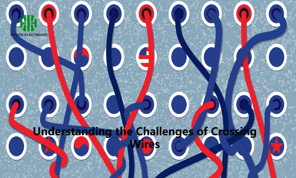
Understanding the Challenges of Crossing Wires
Crossing wires in a PCB design is inevitable, but managing them efficiently can make a significant difference. The key challenges include:
- Crosstalk: When wires carrying different signals are too close, the signals can interfere with each other.
- Signal Integrity: Improper wire crossings can lead to reflections, delays, and signal degradation.
- Electromagnetic Interference (EMI): Crossing wires can become sources of EMI, affecting the performance of the circuit.
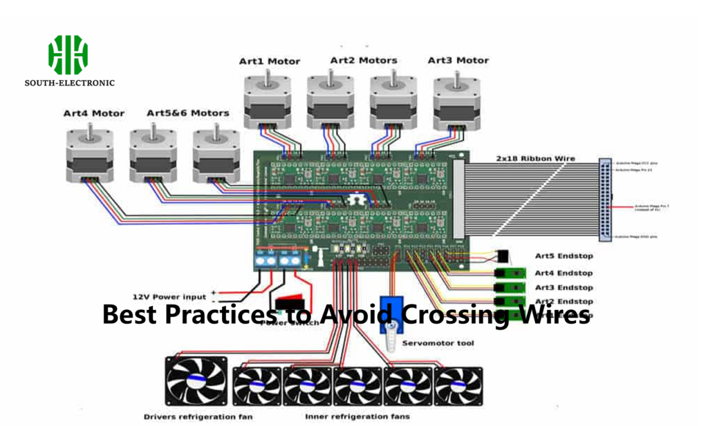
Best Practices to Avoid Crossing Wires
1. Optimize Component Placement
The first step in managing crossing wires is to optimize the placement of components on the PCB. Here are some tips:
- Group Related Components: Place components that are electrically related close to each other to minimize the need for crossing wires.
- Rotate and Reposition Components: Adjust the orientation and position of components to reduce the number of crossings before routing.
Tips for Optimizing Component Placement
| Tip | Description |
|---|---|
| Group Related Components | Keep components that interact closely together to reduce the need for crossing wires. |
| Rotate Components | Rotate components to align their pins for easier routing and fewer crossings. |
| Use Both Sides of the Board | Utilize both the top and bottom layers of the PCB to separate conflicting traces. |
2. Use Multilayer PCBs
For more complex designs, using multilayer PCBs can help in managing crossing wires by providing additional layers for routing. Here’s how:
- Signal Layer Separation: Use different layers for different signal types (e.g., power, ground, signal) to avoid interference.
- Dedicated Ground and Power Planes: Implement dedicated planes for ground and power to reduce noise and improve stability.
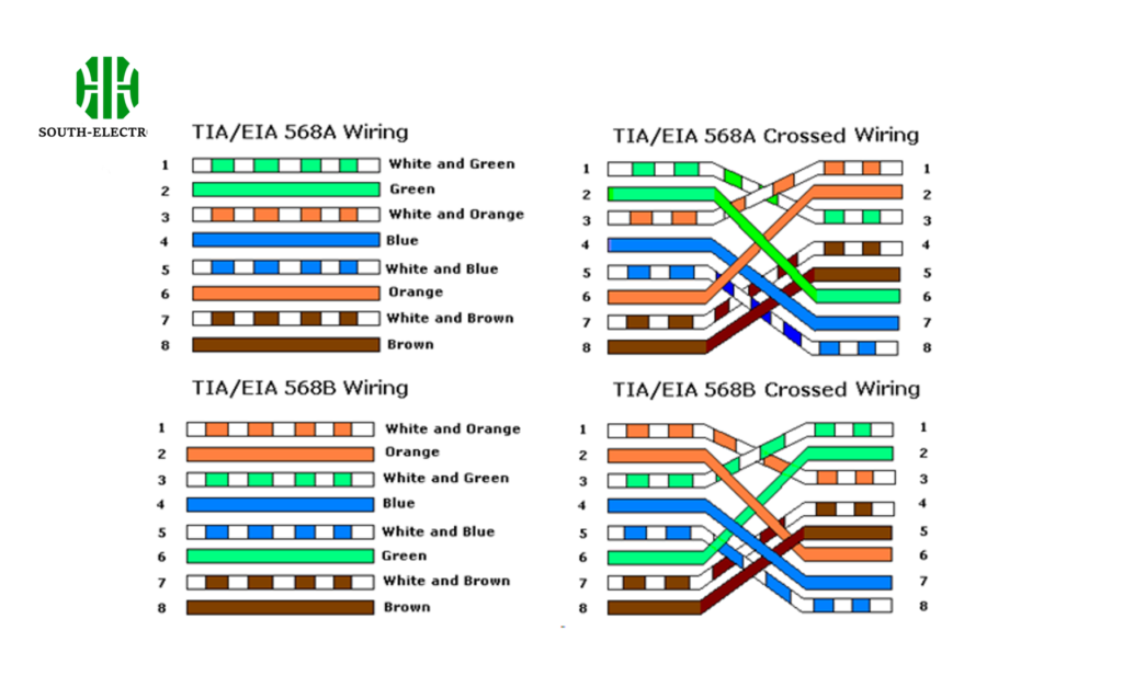
Tools and Techniques for Managing Crossing Wires
1. PCB Design Software with Auto-Routing
Many modern PCB design tools include auto-routing features that can help minimize wire crossings automatically. Popular tools include:
- KiCad: An open-source tool with powerful routing features.
- Altium Designer: Offers advanced auto-routing capabilities for complex designs.
- EAGLE: Known for its user-friendly interface and efficient routing tools.
2. Vias and Jumpers
Using vias and jumpers is an effective way to manage wire crossings by allowing traces to cross without interfering with each other.
- Vias: Small holes that connect different layers of a PCB, enabling traces to pass through layers without crossing.
- Jumpers: Short wires or conductive paths used to bridge over other traces, allowing for cleaner routing.
3. Simulating Wire Crossings with LTspice
LTspice is a great tool for simulating the effects of wire crossings on signal integrity and EMI. By simulating your design, you can find potential issues and optimize your layout before you make it.
Common Mistakes to Avoid
1. Overlooking Ground Loops
Ground loops can cause severe issues in a PCB design, especially when dealing with crossing wires. To avoid ground loops:
- Use Vias Efficiently: Connect components directly to ground points using vias to keep return loops short.
- Isolate Sensitive Signals: Keep sensitive signal paths separate from noisy power or ground planes.
2. Neglecting to Double-Check Connections
Before you finalize your design, always double-check wire crossings and connections. A small mistake can lead to big problems during manufacturing or operation.
Common PCB Design Mistakes and How to Avoid Them
| Mistake | Consequence | Solution |
|---|---|---|
| Overlooking Ground Loops | Signal interference, noise issues | Use vias and keep ground paths short |
| Neglecting to Check Connections | Faulty connections, potential short circuits | Double-check all connections before routing |
| Improper Via Placement | Increased trace length, potential signal delay | Place vias strategically to minimize length |
To make sure your PCB design works right and keeps working right, you need to manage your crossing wires. You can do this by following best practices, using the right tools, and avoiding common mistakes. You should simulate your design, check connections, and use vias and jumpers to minimize crossings.

