
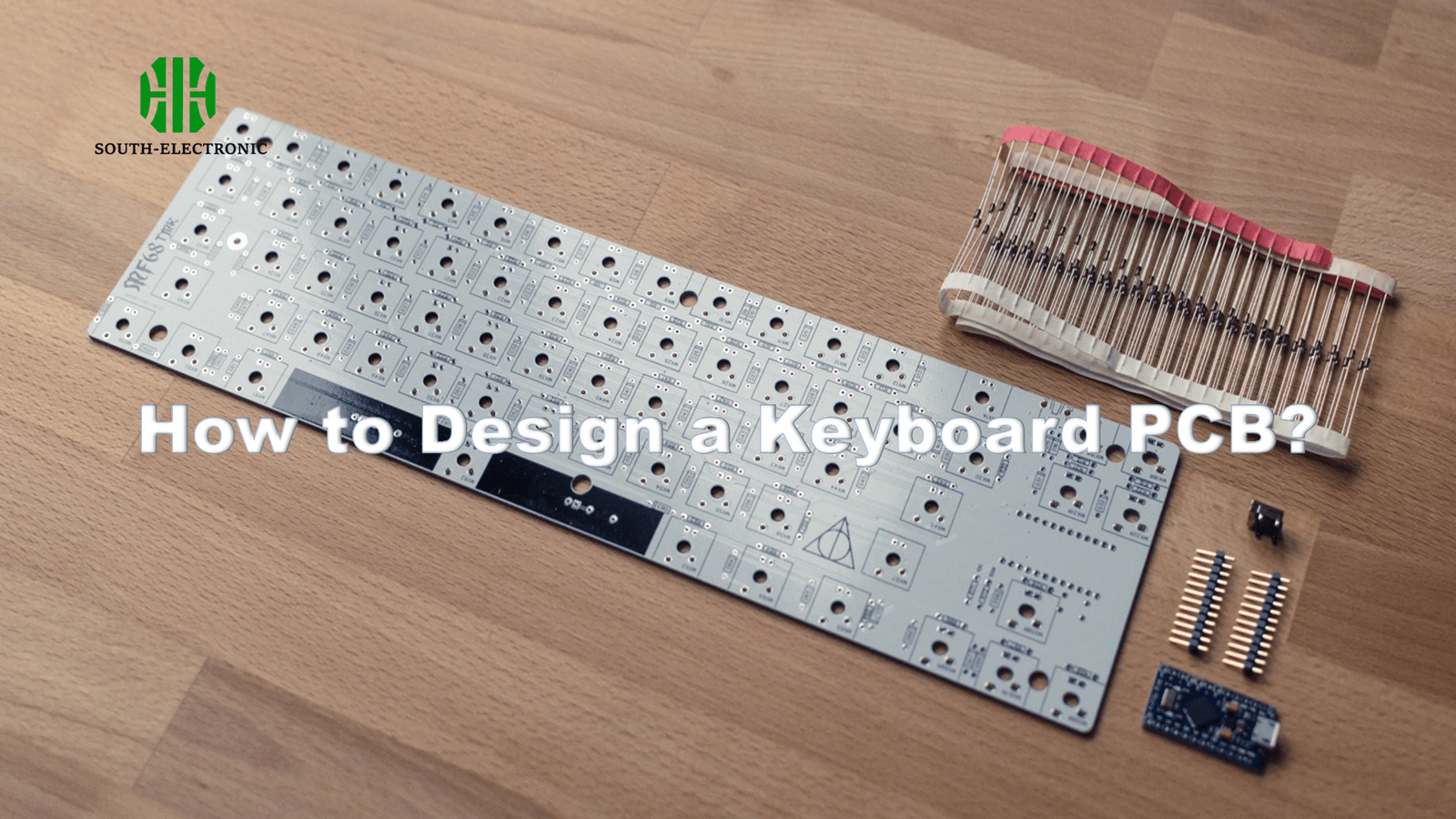
Stuck with generic keyboard limitations? Frustrated by compromises in off-the-shelf kits? I felt that pain until I designed my own PCB. Now I control every aspect of my mechanical keyboard. This solution unlocks true customization freedom.
Designing a keyboard PCB involves planning circuits and routing electrical paths using software like KiCad. I create switch placements and controller connections for personalized layouts. This transforms my unique mechanical keyboard vision into a functional circuit board.
Ready to dive deeper? I’ll guide you through sizing options, connection methods, and sourcing strategies. Each step builds toward your custom keyboard triumph.
What Size Keyboard PCB Do I Need?
Choosing wrong feels awful. Your switches crammed into a mismatched case? My first attempt failed that way. You need precise dimensions aligned to typing habits and desk space.
Keyboard PCB size depends on key count and layout preference. I match sizes like 60% or TKL to daily tasks and case constraints. Always measure physical dimensions first for compatibility. Larger boards offer functionality, while smaller save desk space.
Balancing Key Count and Physical Space
I evaluate my typing needs before choosing keyboard pcbs. Three key factors guide my decisions:
- Layout format: Staggered, ortholinear, or split designs require different PCB shapes
- Key functionality: Dedicated arrows/numpad vs. layer-dependent keys
- Physical constraints: Case dimensions and port placement limitations
This comparison helps visualize tradeoffs:
| Size | Key Count | Ideal For | Space Saving |
|---|---|---|---|
| 60% PCB | 61-64 | Minimalist setups, travel | Best |
| TKL (80%) | 87-88 | Gaming, full functionality | Moderate |
| Full Size | 104-108 | Office work, data entry | Lowest |
| Split PCB | Varies | Ergonomics, custom layouts | Modular |
I test layouts virtually before committing. My daily driver uses a custom 65% PCB – compact yet functional. Split keyboard pcbs solved my wrist pain during long coding sessions. Always prototype with cardboard before ordering PCBs!
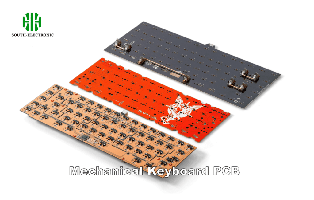
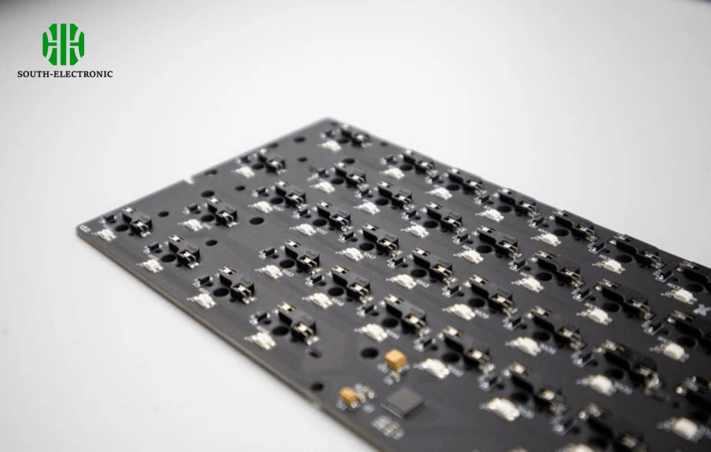
Hot-Swap vs Soldered PCB: Which Keyboard PCB Is Best For YOUR Needs?
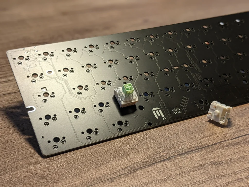
Hate soldering? I burned two boards learning. Hot-swap fixes that frustration. But durability concerns persist. You deserve the right connection method for your typing habits.
Hot-swap sockets allow switch changes without soldering – perfect for experimentation. Soldered joints offer superior permanence and reliability. I assess cost, longevity, and technical comfort first. Builders seeking change flexibility choose hot-swap; stability seekers pick soldered.
Connection Method Breakdown
Hot-swap and soldered keyboard pcbs serve different needs. Critical evaluation reveals these key aspects:
Reliability Factors
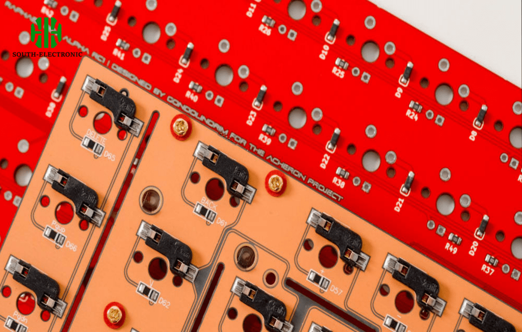
- Kailh sockets in hot-swap boards endure 100+ swaps
- Traditional solder joints typically outlive keyboard housings
- Cold joints in DIY soldering cause premature failures
Usage Scenarios
I choose based on three considerations:
- Switch testing frequency: Constant changes = hot-swap
- Build permanence: Permanent installation = soldered
- Cost: Hot-swap PCBs cost $15-$30 extra
| Flexibility | Durability | Skill Required | |
|---|---|---|---|
| Hot-Swap | Excellent | Good | None |
| Soldered | Poor | Excellent | Medium |
My experimental board uses hot-swap for rapid prototyping. For mechanical keyboard pcbs I depend on daily, I solder everything. First-time builders enjoy hot-swap freedom while learning. Always inspect socket alignment before inserting expensive switches!
Where to Buy Reliable Keyboard PCBs?
Wasting money on dead boards hurts. I threw away $80 on flimsy PCBs before finding trustworthy sources. Bad purchases derail projects and test patience.
Reputable suppliers include KBDFans, CannonKeys, and JLCPCB for custom pcbs. I prioritize manufacturer certifications and customer reviews. Established vendors guarantee compatibility and provide technical support.
Sourcing Strategies Explained
Finding quality custom pcb keyboard components requires smart searching. I categorize sources this way:
Vendor Tiers
- Specialty stores (KBDFans, Mechboards) – Stock popular PCBs
- Group buys – Uniquie designs through Geekhack/Reddit
- Manufacturers (JLCPCB) – Direct fabrication via Gerber files
| Pros | Cons | ||
|---|---|---|---|
| Specialty | Tested products, warranty | Limited designs | $50-$120 |
| Group Buys | Exclusive designs | Long delays | $80-$200 |
| Manufacturers | Full customization | No testing | $20-$50 |
I always request:
- PCB thickness: 1.6mm minimum
- Testing certificates for continuity
- Gold plating for corrosion resistance
My successful 60 keyboard pcb came from KBDFans. For hall effect keyboard pcb experiments, I ordered prototypes from JLCPCB. Avoid untested sellers without community feedback – I learned this through costly mistakes!
Conclusion
Designing your keyboard PCB conquers pre-set limitations. I embrace full creative control through smart sizing, reliable connections, and trustworthy suppliers. Every custom trace reflects personal needs perfectly.


