

Creating a printed circuit board (PCB) without an electrical engineering (EE) background might seem daunting, but with the right tools and guidance, it’s a task anyone can tackle. By following this guide, you can create functional and reliable PCBs.
How to Design a PCB: A Step-by-Step Guide
Printed Circuit Board (PCB) Design is the process of laying out the electrical pathways of a circuit on a board that will support and connect the electronic components. A good PCB design will make your circuit work reliably, reduce the chances of making mistakes, and even make your circuit work better.
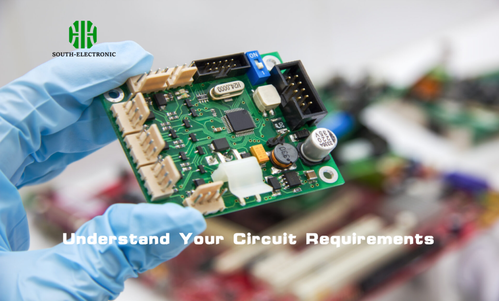
1. Understand Your Circuit Requirements
First, you need to figure out what you want your circuit to do. What problem are you trying to solve? What are the key components you need? You also need to know the electrical parameters, like voltage, current, and what type of components you want to use.
Key Components to Consider:
- Microcontroller/Processor: The brain of your circuit.
- Power Supply: Ensure you have the right voltage and current requirements.
- Input/Output Devices: Sensors, LEDs, and other peripherals.
Pro Tip: Begin with simple circuits. As you gain confidence, you can move on to more complex designs.
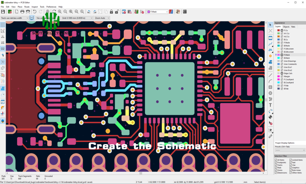
2. Create the Schematic
The schematic is a picture of your circuit. It shows how all the parts are connected. Most PCB design software has a tool that lets you draw the schematic.
Steps to Create a Schematic:
- Place Components: Drag and drop symbols of your components onto the workspace.
- Connect Components: Use lines to represent electrical connections between components.
- Add Labels: Clearly label each component and connection to avoid confusion later.
Tool Recommendation: KiCad is a popular open-source tool that’s great for beginners.
3. Choose Your PCB Design Software
Picking the right software is key, particularly if you don’t have an EE background. Look for software that’s intuitive, well-supported, and has a big user community.
Popular PCB Design Software:
- KiCad: Free and open-source with a rich feature set.
- CircuitMaker: Free but requires registration; great for collaborative projects.
- Eagle: Offers a free version with limited features; widely used in the industry.
Comparison of Popular PCB Design Software
| Software | Price | Ease of Use | Features | Community Support |
|---|---|---|---|---|
| KiCad | Free | Moderate | Advanced features, open-source | Strong |
| CircuitMaker | Free | Easy | Collaboration tools | Active |
| Eagle | Free (Basic) | Moderate | Industry standard, limited free version | Strong |

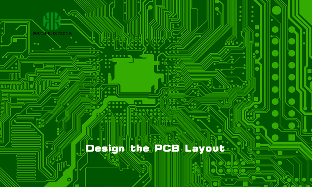
4. Design the PCB Layout
Once you’ve got your schematic finished, the next step is to design the PCB layout. This means you’re going to put your components on the board and then route the electrical connections (traces) between them.
Steps to Design the Layout:
- Place Components: Arrange them logically to minimize trace length.
- Route Traces: Connect components according to the schematic. Prioritize critical signals, like power and ground, first.
- Add Vias and Pads: These are essential for multilayer boards, allowing connections between different layers.
Tool Tip: Many PCB design tools offer auto-routing features, but manual routing gives you more control over the design.
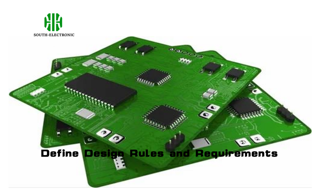
5. Define Design Rules and Requirements
Design rules make sure your PCB works and can be made without problems. These rules cover things like how thin traces can be, how close together traces can be, and how big holes can be.
Common Design Rules:
- Trace Width: Determines the amount of current the trace can carry.
- Spacing: Prevents electrical shorts between traces.
- Via Size: Ensures reliable connections between layers.
Pro Tip: Consult your PCB manufacturer’s guidelines to set these parameters correctly.
6. Simulate and Test Your Design
Before you start manufacturing, it’s important to simulate your PCB design to find and fix any potential problems.
Steps to Simulate:
- Run Electrical Rule Check (ERC): This checks for common schematic errors.
- Perform Design Rule Check (DRC): Ensures your layout adheres to the defined design rules.
- Simulate the Circuit: Some tools allow you to simulate the circuit’s behavior, although this is more advanced and may require additional software.

7. Generate the Gerber Files
Gerber files are the standard format for PCB manufacturing. They have everything you need to make your PCB, like the layout, drilling instructions, and component placement.
Steps to Generate Gerber Files:
- Export from Your Design Software: Most PCB design tools have a built-in function to generate Gerber files.
- Review the Files: Use a Gerber viewer to check the files for any errors.
- Submit to Manufacturer: Once you’re satisfied, submit the files to your chosen PCB manufacturer.
Tip: Double-check the manufacturer’s requirements before submission to avoid delays.

Overcoming Common Challenges in PCB Design Without EE Experience
Designing a PCB without an electrical engineering background can be tough, but if you know what to look out for and how to avoid common mistakes, you can save yourself a lot of time and headaches.
Common Challenges:
- Understanding Electrical Parameters: Start with simple circuits and gradually increase complexity.
- Software Learning Curve: Follow online tutorials and join forums for support.
- Component Placement: Use online resources and reference designs to guide you.
Pro Tip: Practice is key. The more PCBs you design, the more comfortable you’ll become.

Practical Tips to Gain PCB Design Experience
Experience is the best teacher when it comes to PCB design. Here are some tips to accelerate your learning:
Tips for Gaining Experience:
- Start with Kits: PCB kits provide a hands-on way to learn the basics.
- Join Online Communities: Engage with other beginners and experts in forums and social media groups.
- Take Online Courses: Platforms like Coursera and Udemy offer PCB design courses tailored for beginners.
Is It Hard to Design Your Own PCB?
A lot of people think designing a PCB is hard and you have to be some kind of genius engineer to do it. But that’s not true. With the right tools and the right approach, anyone can design their own PCB.
Common Myths:
Myth: PCB Design Requires an EE Degree
Reality: While an EE degree helps, it’s not necessary. Many successful PCB designers are self-taught.
Myth: PCB Design Software is Complicated
Reality: Modern software tools are user-friendly and designed with beginners in mind.

Take Your PCB Design Skills Further
Once you’ve mastered the basics, consider exploring more advanced topics and tools to enhance your skills.
Advanced Resources:
- High-Speed PCB Design: Learn about designing PCBs for high-frequency circuits.
- Multilayer PCB Design: Explore the challenges and techniques for designing multilayer boards.
- Signal Integrity: Understand how to minimize noise and interference in your circuits.
Recommended Courses:
- PCB Design for Engineers and Makers (Udemy): A comprehensive course for intermediate learners.
- High-Speed Digital Design (Coursera): Focuses on the principles of designing high-speed circuits.
You can design a PCB without an EE degree. It’s not only possible, but it’s getting easier every day thanks to modern tools and resources.

