
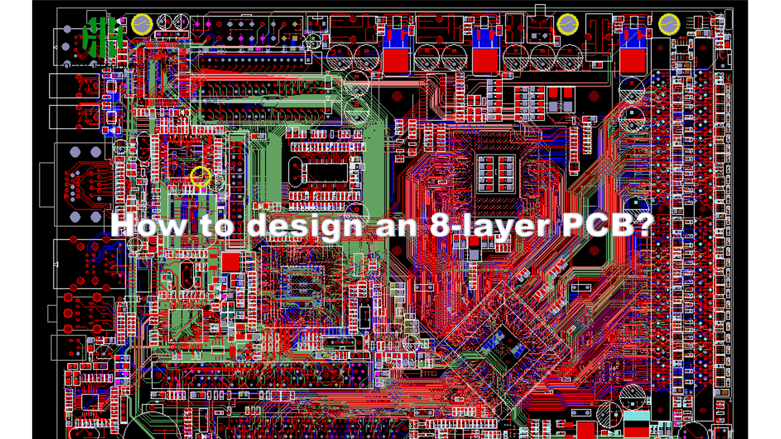
One of the ways to learn PCB design well is to learn the design methods and techniques of predecessors through their works. We can learn component layout, board layer setting, circuit routing from the works of predecessors.
Board layer settings
- Signal layer (TOP)
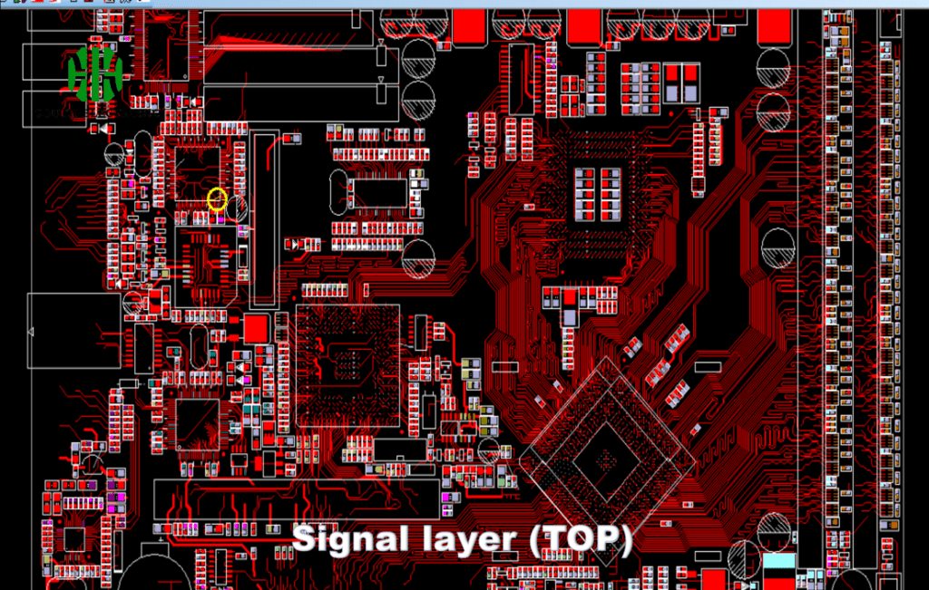
The first signal layer, also called the top layer, is the visible layer when the physical board is printed, and it is the layer where electronic components can be placed. As can be seen from the above picture, there are more wirings on this layer. One of the reasons is that the electronic components are placed on the same layer, and there is no need to set a via conversion layer during the routing process. This can prevent vias from obstructing the routing of other layers. In multi-layer board routing, you should pay attention to the setting of vias.
- Power layer (VCC)
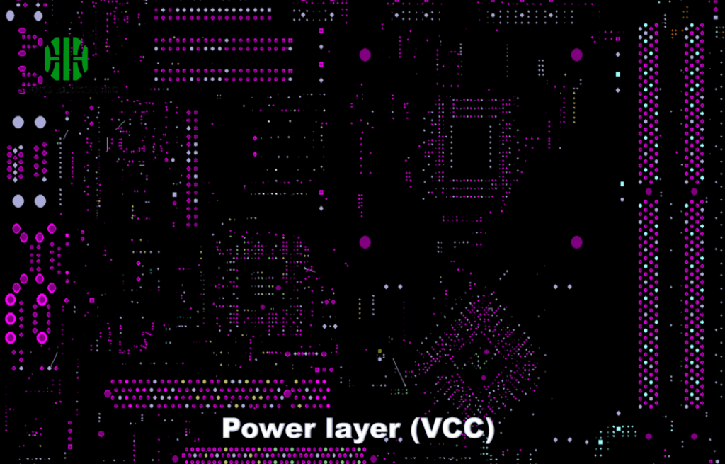
There are no traces on this layer because this layer is all power supply networks. When designing, specific lines are used to divide the power supply. The premise is that when laying out the electronic components, the electronic components with the same voltage must be placed in one area and connected to the same area on this layer through vias, so no traces are needed.
- Signal layer (Inner Layer3)
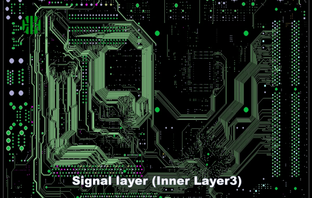
This layer mainly carries signal lines, and also some power lines. The larger lines in the picture below are power lines, and the smaller ones are signal lines.
- Signal layer (Inner Layer 4)
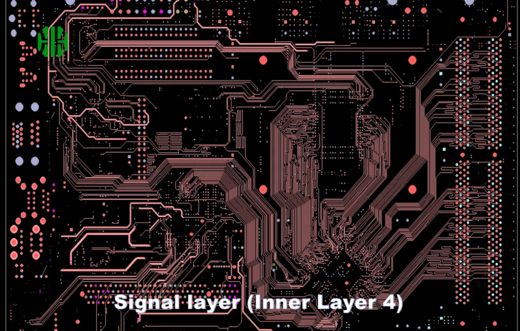
This layer has basically the same routing arrangement as the previous layer. The routing is for signal lines and power lines.
- GND layer
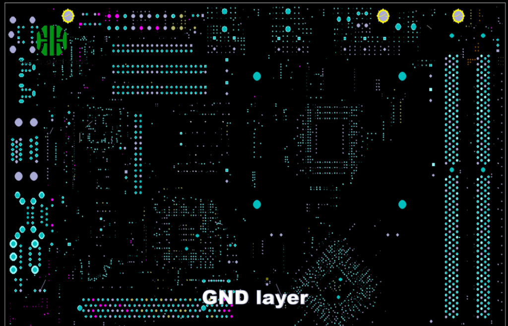
This layer is the GND network layer, connected through vias.
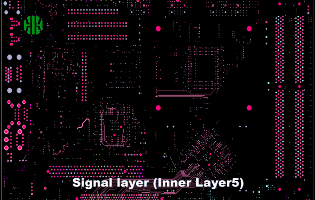
- Signal layer (Inner Layer5)
- GND layer
- Bottom layer
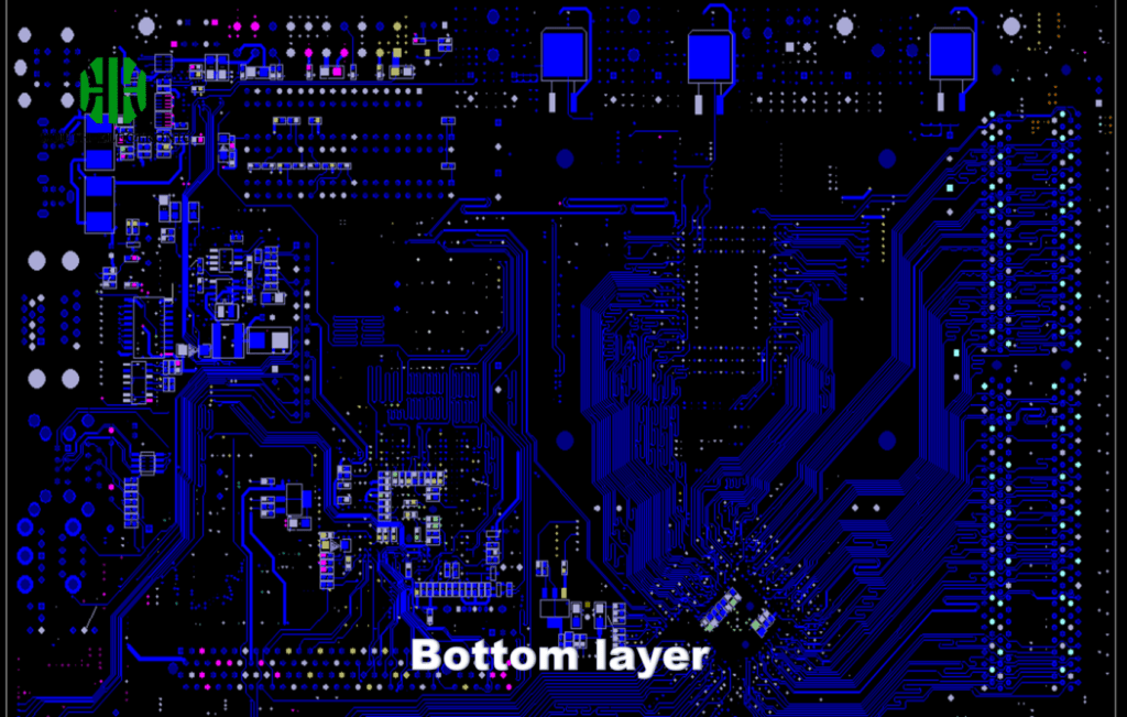
This layer is the same as the top layer. Many small chip routing is basically on the top layer or this layer.
Routing or wiring
- Serpentine routing
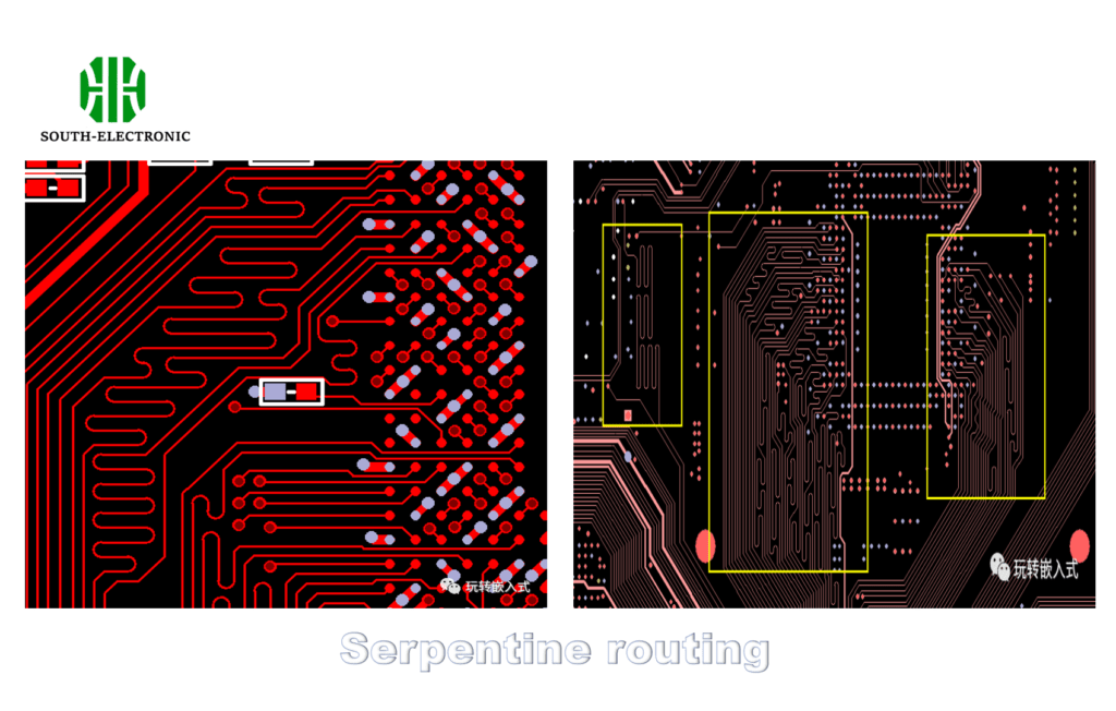
This kind of routing looks pretty. The purpose of this routing is to extend the total length of the routing. It is applied to parallel data lines to make the routing length of the same group of parallel data lines consistent, so that the arrival time of data is consistent when transmitting data at high speed.
The wiring steps of serpentine routing are to first use ordinary routing to route the same group of parallel data lines. Then find the longest line in this group of data lines, and then use the length of the longest line as a reference to extend the line smaller than this reference value through serpentine routing to the same reference value or to a certain range of this reference value. The general circuit board design software has the relevant routing function, and you only need to set the relevant parameters.
- Differential line
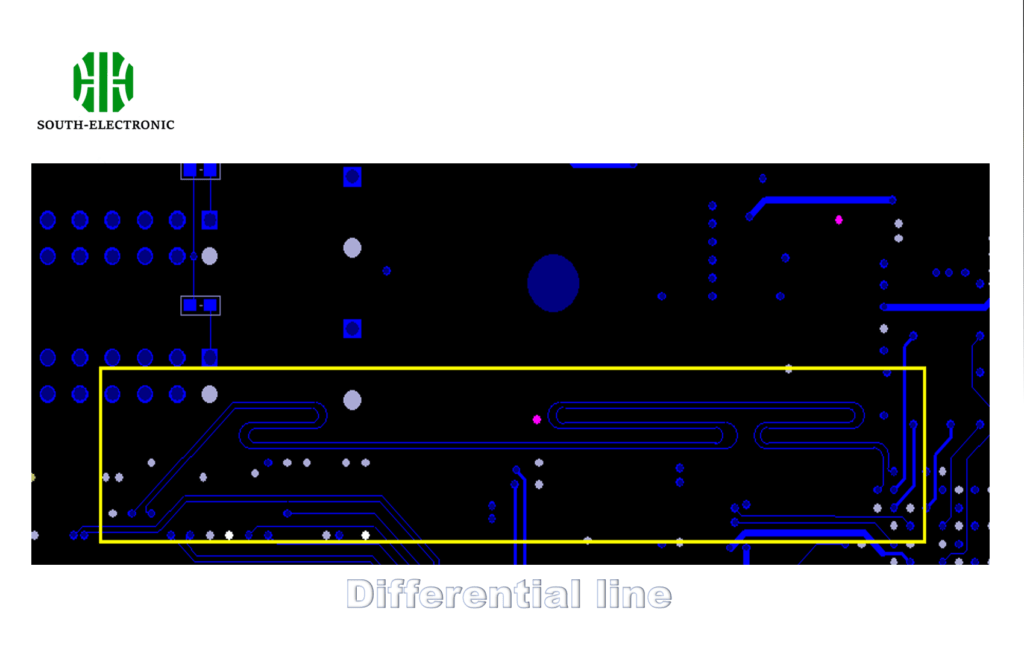
The differential line is actually very similar to the serpentine line above. The serpentine line above is a group of data lines. The differential line only has two lines. However, the requirements are higher and stricter than the serpentine line. Not only must the length of the line be consistent, but the distance between the lines must also be kept at a certain distance. Fortunately, the relevant software has this routing function, and you only need to set the relevant parameters.
- Large or wide routing
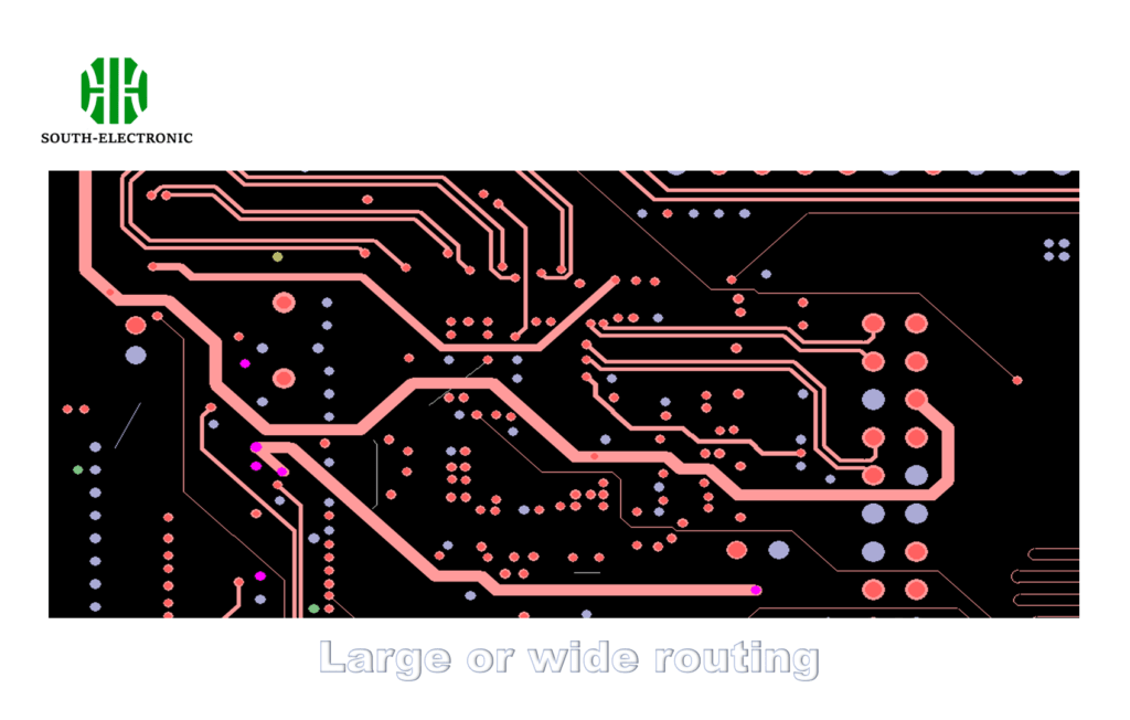
The larger wires in the wiring are usually the power lines, which are related to the component load. The relevant theory will not be elaborated here.
- Component layout
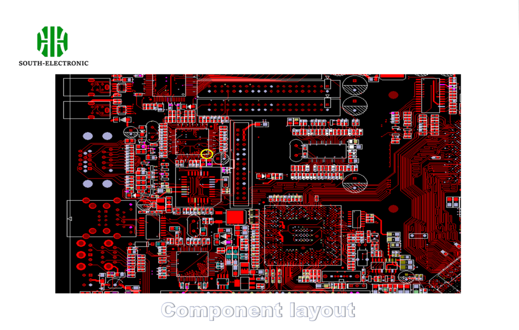
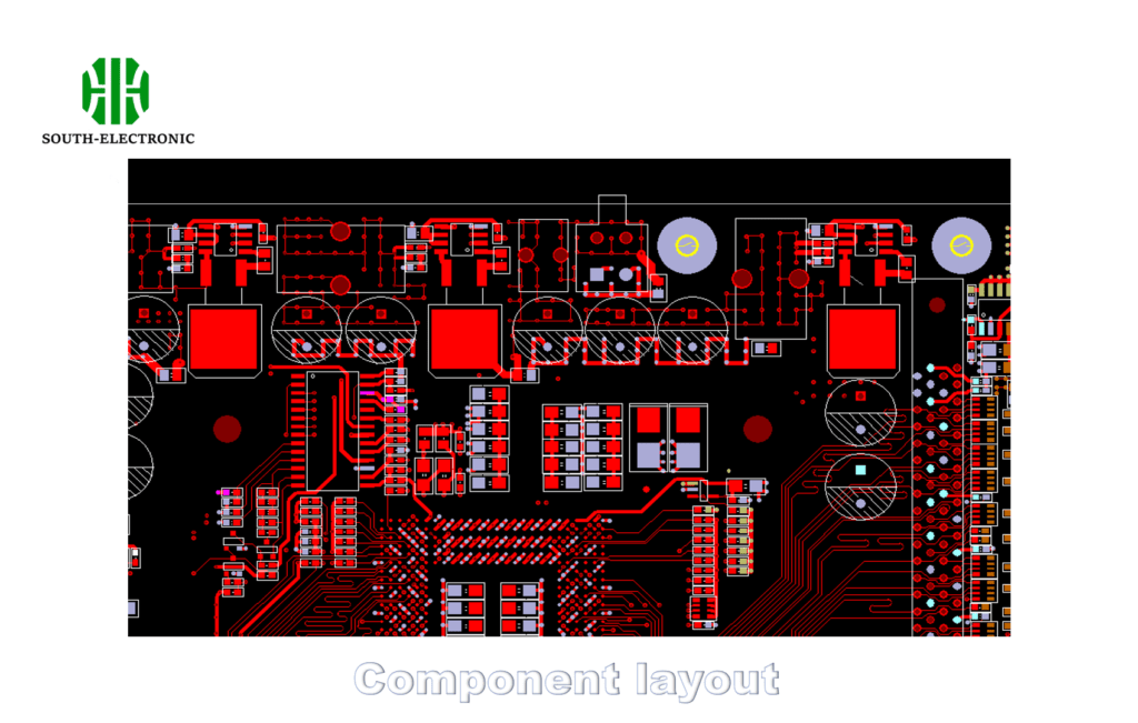
The above is the component layout in the predecessor’s work, isn’t it very nice? The component layout is basically arranged in a modular design. The advantage of this layout is that the related electronic components that realize the same function are arranged together so that the wiring length in the small module can be shorter. When the small module is placed in the large module, it is convenient to frame the complete module. Don’t take too many detours when wiring.


