
Starting your first PCB design feels intimidating. Failed layouts, fried components, and wasted money haunt beginners. But don’t panic — I’ve been there too. Use these proven steps to avoid rookie mistakes.
Designing functional PCBs involves drawing schematics, placing components, and routing connections. Test small batches first to catch flaws early. Free PCB design software makes experimentation affordable and lowers entry barriers.

Ready to move beyond basics? Let’s dissect PCB design fundamentals step-by-step. Each section answers critical questions beginners ask on Reddit and forums.
what is pcb?
Most electronics would be impossible without PCBs. Ever wondered how tiny gadgets manage complex functions? The answer’s etched in layers of copper and insulation.
A PCB (Printed Circuit Board) connects electronic components via conductive copper tracks. It replaces messy wires with printed pathways laminated onto non-conductive material. This design allows compact, reliable circuits in phones, computers, and DIY projects.

Breaking Down PCB Composition
PCBs have layered structures that serve distinct functions. Understanding these helps avoid board failure during fabrication:
| Layer | Material | Function |
|---|---|---|
| Substrate | Fiberglass/FR4 | Provides rigidity & insulation |
| Copper | Thin foil | Forms conductive signal pathways |
| Soldermask | Epoxy polymer | Prevents accidental short circuits |
| Silkscreen | Ink | Labels components & polarity |
Single-layer boards work for basic circuits, like DIY guitar pedals. Multi-layer designs stack copper sheets for complex devices needing dense routing. Always match layer count to project needs — four-layer boards cost more than two-layer ones. High-frequency signals require controlled impedance traces, while power circuits need thicker copper. Poor material choices cause overheating or signal loss. Test prototypes under maximum load to validate thermal performance.
Which Tools Should I Use to Start Learning PCB Design?
Overwhelmed by complex PCB design software options? I nearly quit seeing professional tools costing thousands. Start simple — your wallet will thank you.
Begin with free PCB design software like KiCad or EasyEDA. Their tutorials teach schematic capture and layout routing without cost. These tools handle everything from Arduino shields to Raspberry Pi add-ons, perfect for learning.

Software Guide for Beginners
Online PCB design platforms enable instant collaboration and simulation. Compare key options using these criteria:
| Software | Cost | Key Feature | Best For |
|---|---|---|---|
| KiCad | Free | Multi-layer support | Open-source enthusiasts |
| EasyEDA | Free | Cloud storage & sharing | Collaborative projects |
| Fusion 360 | Paid | CAD integration | Professional mechanical |
| Eagle | Freemium | Extensive part libraries | Hobbyist prototyping |
KiCad works offline for complex designs, while EasyEDA’s web interface simplifies sharing. Use built-in Design Rule Checkers — they catch trace spacing errors before manufacturing. Start with single-sided boards to grasp routing logic. Watch YouTube tutorials on footprint creation; incorrect solder pads cause assembly headaches. Export Gerber files carefully — one format mistake ruins entire batches. Always simulate digital circuits before ordering physical boards.
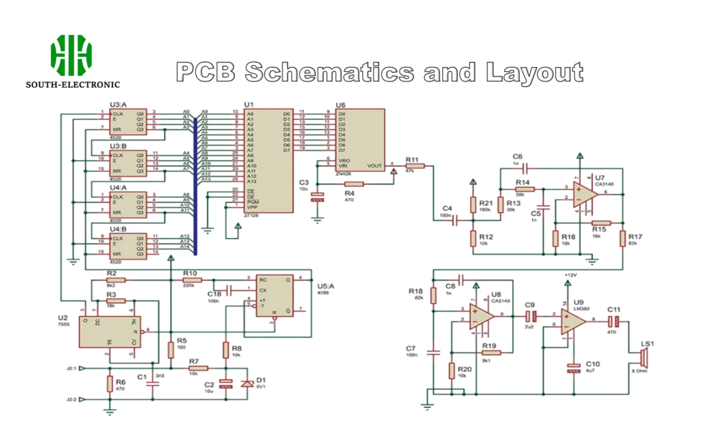
How to Translate a Circuit Schematic into a Practical PCB Layout?
Schematics show logic and connections. But a real PCB requires physical placement magic. I once built a board resembling spaghetti — avoid my chaos.
Convert schematics to layouts by placing high-frequency components first. Minimize path lengths between ICs and connectors. Route power traces wider than signal lines to prevent voltage drops during surges.
Efficient Layout Techniques
Optimize placement and routing with grid-based strategies:
| Stage | Priority | Common Mistake |
|---|---|---|
| Component Placement | Group related parts | Ignoring heat dissipation |
| Power Routing | Short, thick traces | Thin traces causing voltage drop |
| Signal Routing | 45-degree angles | 90-degree bends (causes EMI) |
| Final Check | Clearance verification | Overlooking solder bridges |
Place voltage regulators near power inputs — distance impacts stability. Avoid routing analog and digital traces parallelly; separate them with ground planes. Use vias sparingly — each adds manufacturing costs. Always leave 0.5mm clearance between pads for solder masks. For multi-layer boards, dedicate entire layers to ground/power planes. This controls impedance in high-speed designs like drone controllers. Create test points for oscilloscope probes during troubleshooting.
What should be noted when designing high-speed PCB?
High-speed signals behave unpredictably. My early WiFi module designs failed mysteriously — until I learned signal integrity rules. Simple fixes prevent nightmares.
Prioritize impedance matching with differential pairs for high-speed signals. Use ground planes consistently to shield EMI sources from sensitive components. Minimize vias and abrupt direction changes in GHz-frequency traces.
Critical High-Speed Factors
Signal degradation ruins high-frequency boards like routers or RF modules. Address these factors:
| Challenge | Solution | Design Verification |
|---|---|---|
| Signal Reflections | Controlled impedance routing | TDR measurements |
| Crosstalk | 3x trace spacing | Signal isolation in simulations |
| Power Noise | Decoupling capacitors near ICs | PDN analysis at max load |
| EMI Radiation | Guard traces & shielding cans | Near-field probes testing |
Route USB/HDMI traces as differential pairs with precise length matching. Place decoupling capacitors within 5mm of microprocessor power pins — delayed placement causes voltage spikes. Choose PCB materials with stable Dk values above 4GHz. Simulate eye diagrams for serial links to verify timing margins. For automotive projects, use wider temperature-range FR4 laminates. Test boards inside metal enclosures to replicate real EMI conditions.
Conclusion
Master PCB design through iterative practice. Start simple with online tools, advance to complex layouts, and relentlessly test prototypes. Every board teaches new skills.

