
Modern smartphones pack supercomputer power into pocket-sized devices. But squeezing complex circuitry into shrinking frames creates painful design headaches. The secret lies in balancing aggressive miniaturization with flawless electrical performance—let’s demystify how it’s done.
Efficient mobile PCB design[^1] requires layered strategies: component placement algorithms, signal integrity safeguards, thermal diffusion planning, and military-grade testing protocols. Prioritize space optimization[^2] without compromising reliability—every 0.1mm counts when battling physics in miniature warfare.
Creating a smartphone PCB isn’t just about connections—it’s a survival game against heat, interference, and human error. Below, we dissect four battle-tested tactics that separate functional prototypes from mass-production-ready boards.
What Are the Critical Factors for Efficient PCB Space Optimization in Smartphones?
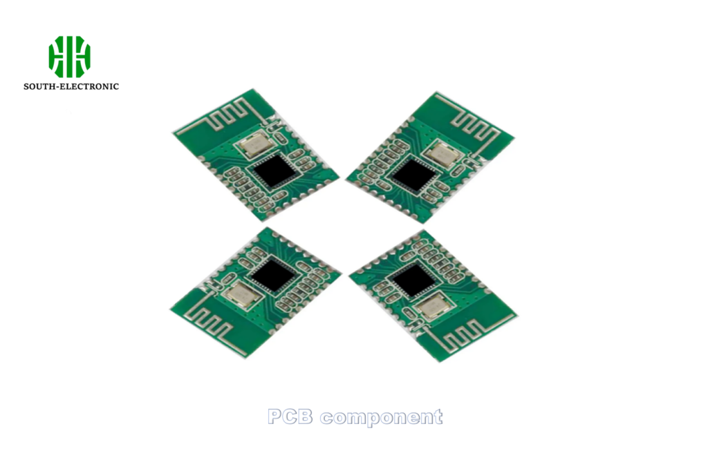
Smartphone PCBs must host 1,000+ components in spaces smaller than credit cards. Poor planning leads to signal crosstalk, overheating, or unfixable design flaws.
Master 3D component stacking[^3] using hybrid rigid-flex boards, laser-drilled microvias, and hexagonal chip arrangements. Allocate 15-20% free space for heat dissipation zones and future revisions—crowded boards fail faster.
Breaking Down Space Optimization
| Strategy | Tools/Techniques | Impact |
|---|---|---|
| Layer Management | 8-12 layer HDI boards | 40% density boost vs 6-layer |
| Component Placement | Auto-router + manual tweaks | Reduces trace length by 22% |
| Flex Integration | Polyimide substrates in bending zones | Survives 200k+ fold cycles |
| Future-proofing | Reserve areas for RF shielding cans | Enables last-minute antenna swaps |
Start with layer stackup planning—mix signal, ground, and power layers strategically. I once saved 2.3mm² by replacing circular chip arrays with hexagonal ones. Use staggered microvias (0.1mm diameter) instead of through-holes for vertical connections. Always cross-check auto-routing results; machines can’t predict finger-induced capacitive coupling near touchscreens.
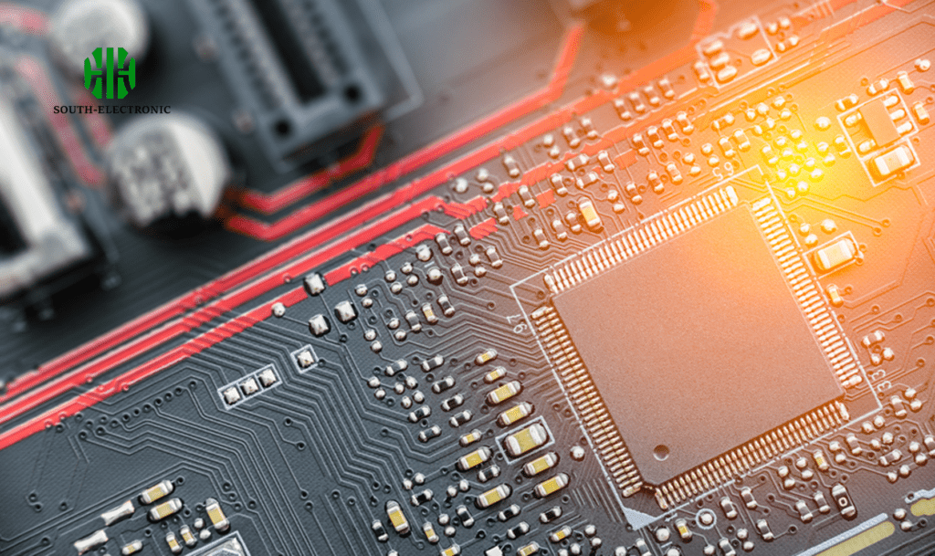
How to Ensure Signal Integrity in High-Speed Mobile Circuits?
Smartphones juggle 5G, WiFi 6E, and UWB signals simultaneously. Uncontrolled EMI turns devices into portable jammers.
Implement differential pair routing[^4] for GHz-speed buses, ground pour isolation between RF modules, and solder mask-defined pads. Perform TDR tests to verify impedance matches[^5]—mismatches over 5Ω cause signal reflections.
Signal Integrity Safeguards
| Risk Factor | Solution | Performance Gain |
|---|---|---|
| Crosstalk | 3W rule (trace spacing ≥ 3x width) | 18dB noise reduction |
| Impedance Drift | Simulated dielectric constants | ±2% impedance control |
| Ground Bounce | Split power planes + decoupling | 30% lower VCC ripple |
| Antenna Coupling | Faraday cage shielding cans | 55dB isolation between radios |
Route DDR4/5 memory lines first—their timing tolerances are tightest. I’ve fixed display flickering by adding ground guards near MIPI DSI lanes. For millimeter-wave antennas (28GHz+), use Rogers 4350B substrates instead of standard FR4 to minimize loss. Always terminate clock lines with characteristic impedance-matched resistors.
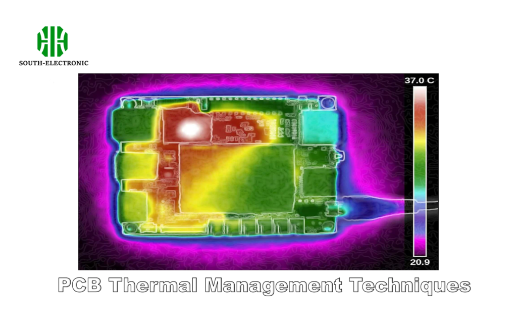
Why Is Thermal Management a Lifesaver for Mobile PCB Longevity?
A smartphone SOC can hit 110°C during gaming—enough to melt solder joints. Without heat dissipation, your $1k phone becomes a paperweight in 6 months.
Deploy copper-filled thermal vias under hot chips, graphite heat spreaders, and phase-change thermal pads. Keep component junctions below 85°C—every 10°C drop doubles lifespan.
Cooling Techniques Compared
| Method | Best For | Thermal Resistance (°C/W) |
|---|---|---|
| Thermal Vias Array | CPU/GPU hotspots | 15-20 |
| Heat-Spreading Foils | Battery/PMIC areas | 25-30 |
| Liquid Crystal Polymer | RF Front-end modules | 40+ |
| Air Gap Insulation | Camera sensors | 50+ |
Place temperature sensors near PMICs and charging ICs—they’re failure hotspots. During a tablet project, using 576 thermal vias under the SOC lowered peak temps by 14°C. Avoid metal shields over WiFi/BT modules—they trap heat. Instead, use laser-ablated polymer shields with micro-venting holes.
What Testing Methods Guarantee Robust Mobile PCB Functionality?
60% of field failures stem from undetected design flaws. Comprehensive testing catches ghosts in the machine before mass production.
Combine automated optical inspection (AOI)[^6], flying probe tests, and thermal shock cycling[^7]. For mission-critical boards, use SYSCAN JFU-5200 for 360° JTAG boundary scans—it finds 99.97% of latent defects.

Test Protocol Breakdown
| Test Stage | Equipment Used | Checks Performed |
|---|---|---|
| Pre-Assembly | X-ray inspection | Microvia integrity |
| Post-SMT | 3D AOI machines | Solder paste volume |
| Functional Testing | DC Load Analyzers | Power rail stability |
| Environmental | Thermal Shock Chamber | -40°C to 125°C cycle survival |
| Field Simulation | Drop Testers (1.5m height) | BGA joint durability |
During audio module testing, I discovered coil whine only when probing at 200MHz bandwidth. Always test charging circuits with mismatched cables—users will. For waterproof phones, conduct ionic contamination tests after conformal coating. Budget 14% of project time for design validation—it prevents 90% of recall risks.
Conclusion
Mastering mobile PCB design demands precision warriorship—optimize spaces like Tetris, shield signals like Faraday, cool components like refrigerators, and test like paranoid scientists. Future-proof your boards, because tomorrow’s tech fits in yesterday’s footprints.
[^1]: Explore this resource to understand the latest techniques and strategies for optimizing PCB design in smartphones, ensuring reliability and performance.
[^2]: Discover effective strategies for space optimization in smartphone PCBs to avoid design flaws and improve performance in compact designs.
[^3]: Learn about the advantages of 3D component stacking in PCB design, which can significantly enhance space efficiency and thermal management.
[^4]: Understanding differential pair routing can significantly enhance your circuit design, ensuring better signal integrity and performance.
[^5]: Learning about impedance matching is crucial for optimizing signal integrity and minimizing reflections in your designs.
[^6]: Explore this link to understand how AOI enhances PCB testing efficiency and accuracy, ensuring high-quality production.
[^7]: Learn about thermal shock cycling to see how it tests PCB durability under extreme conditions, crucial for reliable performance.

