

BGA packages intimidate many designers. Escape routing nightmares, thermal chaos, hidden solder defects. I spent nights troubleshooting BGA failures before mastering solutions. This guide saves you that pain.
Designing perfect BGA footprints requires proper pad sizing, solder mask control, via placement, and thermal relief per IPC-7351 standards. Select dimensions based on ball pitch and package tolerances to prevent bridging or opens.

Mastering the land pattern is just the start. Dense packages introduce complex routing puzzles and thermal challenges. Worse, hidden solder defects can escape production checks. Let’s tackle these critical issues step by step.
What are BGA escape routing strategies[^1] and microvia essentials for dense packages?
Ever face impossible routing in tight BGA pitch zones? Signals get trapped, layer counts explode. I’ve scrapped boards due to escape routing failures. Don’t repeat my mistakes.
Escape routing uses microvias for high-density interconnects. Place vias between pads in dog-bone patterns. Stagger microvias across layers for congestion relief while maintaining signal integrity.
Advanced Techniques for Complex Packages
Escape routing demands planning before layout. Break options into three approaches:
| Routing Priority Groups | Priority | Signals | Strategy |
|---|---|---|---|
| 1 | Power/Ground | Direct vertical connections | |
| 2 | High-speed | Short paths with impedance control | |
| 3 | General I/O | Peripheral routing paths |
Start with via-in-pad for thermal pads – it saves space but costs more. For signal balls, use dog-bone traces to offset microvias. Always check manufacturability: avoid drill aspect ratios over 8:1. I add 0.1mm capture pads around microvias for reliability.
Layer Stackup Planning
Distribute fan-out layers equally. A 4-layer escape needs:
- Layer1: Microvias + short traces
- Layer2: Horizontal routing
- Layer3: Vertical routing
- Layer4: Escape channels
This prevents overlap. Use solder mask plugs in unused vias to prevent wicking issues. Remember, dense packages require trace/space values below 100μm. Negotiate this early with your PCB fab.
Via Management Basics
Microvias solve routing but introduce risks. Standard microvias handle most needs. Stacked microvias increase reliability for high-stress areas. Stick to 0.1mm diameter when space allows. Always perform signal integrity checks after routing. I simulate with at least 3mm escape channels before committing.
How does BGA heat up and cool down? How to manage its thermal performance[^2]?
Feel that BGA getting hot? Heat sinks won’t save you here. I’ve seen packages desolder themselves during testing. Thermal runaway kills reliability silently.
BGAs heat from current flow through resistance. Cooling happens through conduction into the PCB. Manage thermal resistance with special pad designs, copper balancing, and strategic airflow control.
Thermal Optimization Tactics
Controlling BGA temperatures rests on three pillars:
| Conduction Path Engineering | Method | Implementation | Impact |
|---|---|---|---|
| Thermal vias | Grid under hot components | 30-40% heat reduction | |
| Copper zones | Connect pads to internal planes | Spreads heat laterally | |
| Metal-core boards | Insulated metal substrates | High-cost solution |
Place thermal vias directly under hot spots in 0.5-1mm grid patterns. Filled vias conduct best. I specify 0.3mm vias with copper fill for demanding chips. Balance copper distribution – asymmetric planes cause warping.
Material Selection Factors
Standard FR-4 conducts poorly. Alternatives:
- High-thermal-conductivity substrates
- Metal-clad laminates
- Thermal adhesives
For extreme needs, I choose aluminum-backed boards. They triple heat dissipation but hike costs. Verify your solder paste survives the coefficient mismatch. Always model thermal expansion in CAD tools.
Convection & Software Tools
Forced airflow helps but has limits:
- Position BGAs upstream from heat sources
- Use thermal pads to case interiors
- Add heatsinks with low-profile fins
Simulate early with tools like Ansys Icepak. I log temperature at multiple package corners. Aim for under 100°C at hottest points. Remember local heating near vias!
How to assure BGA package and solder joint quality[^3] beyond X-ray inspection?
X-rays miss crucial defects. I recall a batch passing X-ray but failing in-the-field. Voids hide while cracks spread silently. Standard checks aren’t enough.
Go beyond X-ray with CT scanning, destructive testing, and boundary scans. Monitor thermal cycling performance. Examine solder alloy compositions to prevent brittle joints proactively.
Comprehensive Quality Framework
Build reliability from design to testing:
Pre-Production Controls
| Stage | Action | Target |
|---|---|---|
| Design Review | Model pad stress points | Prevent tear failure |
| DFM Check | Validate fab capabilities | Eliminate yield killers |
| Stencil Design | Optimize aperture ratios | Control solder volume |
Specify solder paste alloys carefully. Lead-free SAC305 works generally but consider low-silver alloys for shock resistance. I mandate IST (interconnect stress test) data from suppliers before approval.
Advanced Inspection Techniques
Combine complementary methods:
- Acoustic microscopy finds de-lamination
- Cross-sectioning measures void percentage
- CT scanning reveals 3D internal defects
- Dye penetration identifies micro-cracks
Prioritize CT scanning for mission-critical assemblies. I use automated optical inspection (AOI) for surface clues: discoloration flags solderability issues.
Reliability Testing Protocol
Simulate real-world conditions:
- Thermal cycling (-40°C to +125°C)
- Mechanical shock testing (1500G impacts)
- Vibration endurance (10-2000Hz sweeps)
Track failure modes using Weibull analysis. I demand 500+ thermal cycles before sign-off. Log all cracked joints to refine designs incrementally.
Can broken BGAs be fixed?
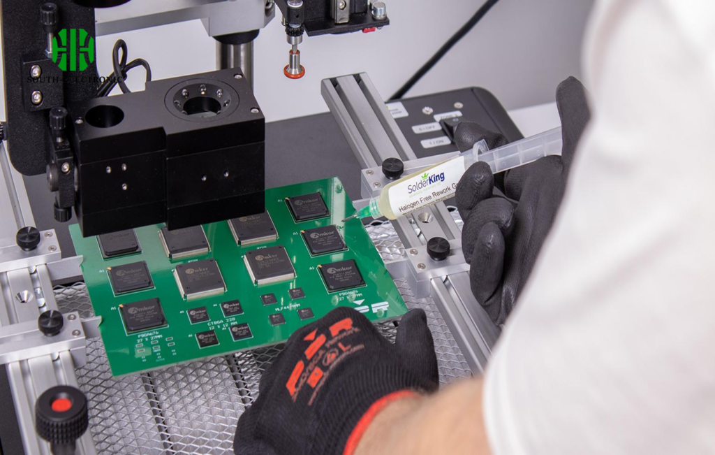
Failed BGAs aren’t always trash. I’ve rescued prototype boards through rework. But poorly handled repairs worsen damage. Know when and how to repair properly.
Professional rework stations can replace broken BGAs. Success depends on heating uniformity, alignment precision, and flux selection. Consider costs: rework often exceeds 50% of board value.
Rework Procedure Breakdown
Effectively repair BGAs through five phases:
Damage Assessment
Determine feasibility:
- Cracked substrates: Unrepairable
- Damaged pads: Possible with trace repair
- Internal failures: Replacement required
Use microsectioning to inspect layers. I reject repairs requiring over 3 pad rebuilds – reliability drops sharply. Estimate time/cost before proceeding.
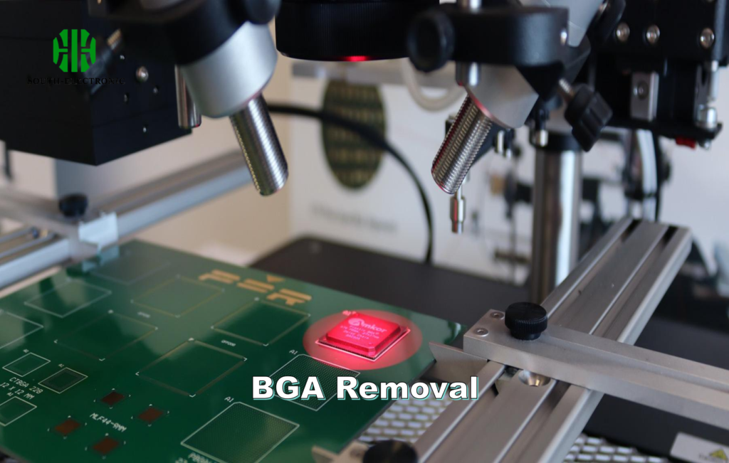
| Controlled Removal Process | Step | Tool/Condition | Risk Control |
|---|---|---|---|
| Preheat | Bottom heater 100-150°C | Prevent warping | |
| Main heating | Nozzle + IR at 240-260°C | Shield nearby components | |
| Lift-off | Vacuum pen at 0.5mm/s | Avoid pad tearing |
Record thermal profiles! I save successful curves for each package size. Post-removal, clean using wick braid with extra flux. Never scratch pads.
Replacement Protocol
- Apply tacky flux
- Ball-align with stencils
- Reflow using gradual ramping
- Hold at liquidous for full wetting
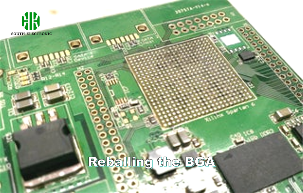
Pre-balled components save time. For specialty BGAs, I stencil-print solder then reball manually. Verify coplanarity under 0.15mm across all balls.
Verification & Acceptance
Post-reflow inspection includes:
- X-ray alignment confirmation
- Continuity checks (all nets)
- Functional testing at temperature extremes
I stamp reworked boards and log hours for reliability tracking. Never use reworked units in flight-critical applications.
Conclusion
Perfect BGA footprints blend pad precision with escape routing strategies, thermal controls, quality testing, and rework knowledge. Master these areas for reliable high-density designs.
[^1]: Explore this resource to learn advanced techniques for BGA escape routing that can enhance your PCB design efficiency and reliability.
[^2]: Understanding thermal performance management is crucial for preventing overheating in BGAs. This resource will provide essential strategies for effective thermal control.
[^3]: Discover comprehensive methods to assure solder joint quality beyond standard inspections, ensuring long-term reliability in your designs.

