

Ever stared at a blank PCB design interface, paralyzed by "what comes next"? I’ve been there. Designing my first board felt like assembling IKEA furniture without instructions—until I cracked this 4-step formula.
PCB design becomes manageable when broken into schematic capture, layout planning, component placement, routing, DRC validation, prototyping, and Gerber file generation. This workflow balances technical precision with real-world manufacturing needs for first-timers.
Many guides overwhelm beginners with jargon-heavy explanations. Let’s cut through the noise with actionable steps paired with pro-tested strategies—no electrical engineering PhD required.
Understanding PCB Design Fundamentals: Schematics vs. Layouts?
Your blinking LED project just fried because schematics and layouts were mixed up. I learned this truth through crispy resistors and smoke signals.
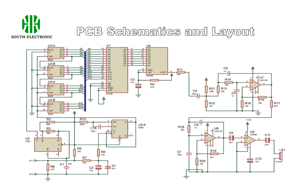
Schematics define electrical connections logically, while layouts physically arrange components on the board—like architectural blueprints versus actual construction plans. Confusing them causes short circuits and non-functional boards.
)
Two Sides of the Same Board
| Feature | Schematics | Layouts |
|---|---|---|
| Focus | Logical connections | Physical placement |
| Tools Used | Symbol libraries | Footprint libraries |
| Critical Metrics | Circuit functionality | Signal integrity, EMI |
| Validation | ERC (Electrical Rule Check) | DRC (Design Rule Check) |
Schematics use abstract symbols to map component relationships, ignoring physical sizes. Layouts demand millimeter-level precision for traces and pads. Beginners often skip ERC checks in schematics, then wonder why their layouts fail DRC. Master this duality early to avoid redesign loops.
Step 1: Choosing the Right EDA Tool – Free vs. Professional Options?
EDA tool paralysis kills more PCB projects than faulty traces. My first month’s tool-hopping delayed three projects before I cracked the selection code.
Free tools like KiCad suit hobbyists/simple boards, while Altium Designer or Cadence streamline complex projects—but overpaying for unused features burns budgets fast.
)
Tool Selection Decoded
| Factor | Free Tools (KiCad, EasyEDA) | Paid Tools (Altium, OrCAD) |
|---|---|---|
| Learning Curve | Steeper (DIY documentation) | Smoother (Official tutorials) |
| Advanced Features | Limited simulation/analysis | Full DFM, 3D EMI analysis |
| Collaboration | Basic version control | Real-time team editing |
| Cost | $0 (Open-source) | $2,000+/year per license |
Choose based on project complexity: 2-layer Arduino shield? KiCad wins. 12-layer medical device PCB with impedance control? Altium’s worth the investment. I use free tools for 80% of personal projects, reserving professional suites for client work with tight tolerances.
Step 2: Component Placement – Avoiding Thermal and Signal Integrity Pitfalls?
That 5V regulator melted your PCB? Mine too, until I stopped treating placement like a game of Tetris.
Component placement dictates thermal performance and signal quality. Poor arrangement causes overheating, crosstalk, and EMI failures—issues found in 37% of first-attempt boards (IPC survey data).
)
Strategic Placement Framework
| Zone | Components | Placement Rules |
|---|---|---|
| Power Section | Regulators, converters | Board edges, near input/output |
| High-Speed | MCUs, memory chips | Shortest possible clock traces |
| Analog | Sensors, op-amps | Isolated from digital noise |
| Thermal | Heatsinks, high-power ICs | Adequate airflow spacing |
Group components by function and thermal needs. Place power elements first, followed by critical ICs. Leave 3-5mm clearance around heat-generators. For analog circuits, create moats (ground gaps) between digital sections. I use colored post-its to map zones physically before clicking in components.
Step 3: Design Rule Check (DRC) – Your Manufacturing Safety Net?
My first DRC failure cost $480 in scrapped boards. Now I run 12 custom DRC profiles matching different manufacturers’ capabilities.
DRC validates trace widths, clearances, hole sizes against your fab’s specs—detecting 89% of manufacturing showstoppers pre-production (MacroFab analysis).
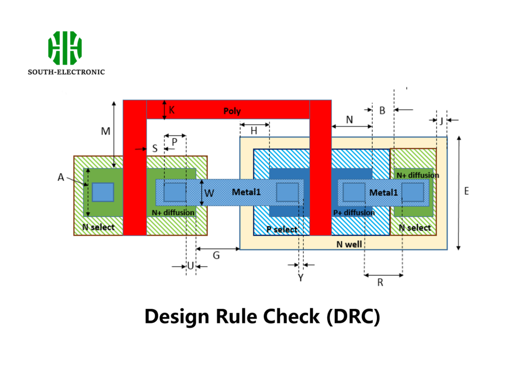
DRC Configuration Checklist
| Rule Type | Standard Value | Criticality |
|---|---|---|
| Minimum Trace | 0.2mm (8mil) | High – Breakout failures |
| Clearance | 0.15mm (6mil) | High – Short circuits |
| Via Diameter | 0.3mm drill / 0.6mm pad | Medium – Drill breakage |
| Silk Text Height | 0.8mm | Low – Legibility issues |
Always request your manufacturer’s DRC file before starting layouts. I create a "DRC Triad": Manufacturer Rules (hard limits), Best Practices (0.25mm traces for power), and Project-Specific (2mm clearance for 1kV sections). Run DRC after every major layout change.
Step 4: Generating Gerber Files – What Manufacturers Actually Need?
That sinking feeling when the fab emails “missing .GKO file”? I’ve refreshed my inbox in panic too. Now my Gerber checklist prevents 100% of these issues.
Manufacturers need 9 Gerber files + drill data: copper layers, solder mask, silkscreen, board outline, and NC drill—omitting any causes production delays.
Gerber File Master List
| File Type | Extension | Contains |
|---|---|---|
| Top Copper | .GTL | Component-side traces |
| Bottom Copper | .GBL | Solder-side traces |
| Top Solder Mask | .GTS | Exposed pads (green layer) |
| Board Outline | .GKO/GML | Cut lines for PCB shape |
| NC Drill | .TXT | Hole locations/sizes |
Use ViewMate or online Gerber viewers to verify layers. Pro tip: Name files clearly (ProjectX_TopCopper.GTL) and zip with a README.txt explaining layer purposes. I email myself zipped Gerbers to check mobile rendering—if I can’t recognize layers on a phone screen, my fab definitely can’t.
Conclusion
From schematics to Gerbers, PCB design challenges crumble with structured steps. Master the EDA tool duality, strategic placement, and manufacturing checks—your first functional board is four focused steps away. Now go etch that idea into reality.

