

As a PCB design engineer, it is a hard requirement to have relevant design capabilities. These essential capabilities include PCB layout, PCB stackup design, power ground processing, DDR signal routing, high-speed signal routing, key signal routing, DRC inspection, etc. Today, I will share with you: PCB stackup design.
PCB stackup design
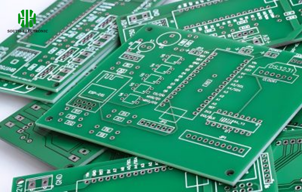
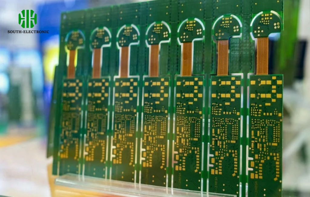
The number of layers of a PCB depends on the complexity of the circuit board. From the perspective of the PCB processing process, a multi-layer PCB is manufactured by stacking and pressing multiple "double-sided PCBs". However, the number of layers of a multi-layer PCB, the stacking order between layers, and the selection of board materials are determined by the circuit board designer, which is the so-called "PCB stackup design".
PCB design engineer capability requirements: be able to master the composition of PCB stackup, master the requirements of stackup design, be able to use tools for stackup design and impedance calculation control, and master the basic principles of PCB stackup settings.
The number of layers and stacking scheme of a PCB design depends on the following factors:
-
Hardware cost: The number of PCB layers is directly related to the final hardware cost. The more layers, the higher the hardware cost. Hardware PCB represented by consumer products generally has a maximum limit on the number of layers. For example, the number of PCB layers of the motherboard of notebook computer products is usually 4 to 6, and rarely exceeds 8 layers;
-
The output of high-density components: For high-density components represented by BGA packaged devices, the number of output layers of such components basically determines the number of wiring layers of the PCB board;
-
Signal quality control: For PCB designs with relatively concentrated high-speed signals, if you focus on signal quality , then it is required to reduce the adjacent layer wiring to reduce the crosstalk between signals. At this time, the ratio of the number of wiring layers to the number of reference layers (Ground layer or Power layer) is preferably 1:1, which will increase the number of PCB design layers; on the contrary, if there is no mandatory requirement for signal quality control, the adjacent wiring layer solution can be used to reduce the number of PCB layers;
-
Schematic signal definition: The schematic signal definition will determine whether the PCB wiring is "smooth". Poor schematic signal definition will lead to unsmooth PCB wiring and increase the number of wiring layers;
-
PCB manufacturer processing capability baseline: The stacking design scheme (stacking method, stacking thickness, etc.) given by the PCB designer must fully consider the PCB manufacturer’s processing capability baseline, such as: processing flow, processing equipment capabilities, common PCB board models, etc.
General principles of PCB stacking design
Meet the characteristic impedance requirements of the signal; meet the principle of minimizing the signal loop; meet the requirements of minimizing signal interference within the PCB; meet the principle of symmetry.
Specifically, PCB engineers need to pay attention to the following 9 aspects when designing multilayer boards:
-
A signal layer should be adjacent to a copper layer, and the signal layer and the copper layer should be placed at intervals. It is best that each signal layer can be adjacent to at least one copper layer. The signal layer should be tightly coupled with the adjacent copper layer (that is, the dielectric thickness between the signal layer and the adjacent copper layer is very small).
-
The power copper and the ground copper should be tightly coupled and in the middle of the stack. Shortening the distance between the power and ground layers is conducive to the stability of the power supply and reducing EMI. Try to avoid sandwiching the signal layer between the power layer and the ground layer. The close proximity of the power plane and the ground plane is like forming a flat capacitor. The closer the two planes are, the greater the capacitance value. The main function of this capacitor is to provide a low-impedance return path for high-frequency noise (such as switching noise), so that the power input of the receiving device has smaller ripples and enhances the performance of the receiving device itself.
-
In the case of high speed, extra ground layers can be added to isolate the signal layer. Multiple ground copper layers can effectively reduce the impedance of the PCB and reduce common-mode EMI. However, it is recommended not to add more power layers for isolation, which may cause unnecessary noise interference.
-
The high-speed signals in the system should be in the inner layer and between the two copper foils, so that the two copper foils can provide shielding for these high-speed signals and limit the radiation of these signals to the two copper foil areas.
-
Give priority to the transmission line model of high-speed signals and clock signals, design a complete reference plane for these signals, and try to avoid crossing the plane partition area to control the characteristic impedance and ensure the integrity of the signal return path.
-
The situation where two signal layers are adjacent. For boards with high-speed signals, the ideal stacking is to design a complete reference plane for each high-speed signal layer, but in practice we always need to make a trade-off between the number of PCB layers and the PCB cost. In this case, it is inevitable that there are two adjacent signal layers. The current practice is to increase the spacing between the two signal layers and make the routing of the two layers as vertical as possible to avoid signal crosstalk between layers.
-
It is best to set copper layers in pairs. For example, the 2nd and 5th layers or the 3rd and 4th layers of a six-layer board should be coppered together. This is to take into account the requirements of balanced structure in the process, because unbalanced copper layers may cause warping and deformation of the PCB.
-
The secondary surface (i.e. the layer close to the surface) is designed as a ground layer, which is conducive to reducing EMI.
-
Estimate the number of required signal layers based on the PCB device density and pin density, and determine the total number of layers.
When actually carrying out stacking design, PCB design engineers need to flexibly apply the above principles and select the most appropriate board layer structure according to the actual system requirements.

