

How can we optimize PCB design to reduce the risk of shorts and opens?
To optimize PCB design and reduce the risk of shorts and opens, we must first control the source. Starting from the design, we can improve the following aspects:
- Maintaining Sufficient Clearance:
When designing a PCB, ensure sufficient clearance between traces and vias to prevent shorts. It’s generally recommended to set the clearance equal to or greater than the minimum positive trace width that the PCB manufacturer can etch. Furthermore, in high-density designs, sufficient buffer space should be left between pads to prevent solder from overflowing and affecting nearby pads.
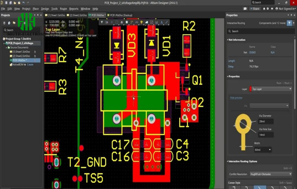
- Properly Set Pad Spacing and Line Width:
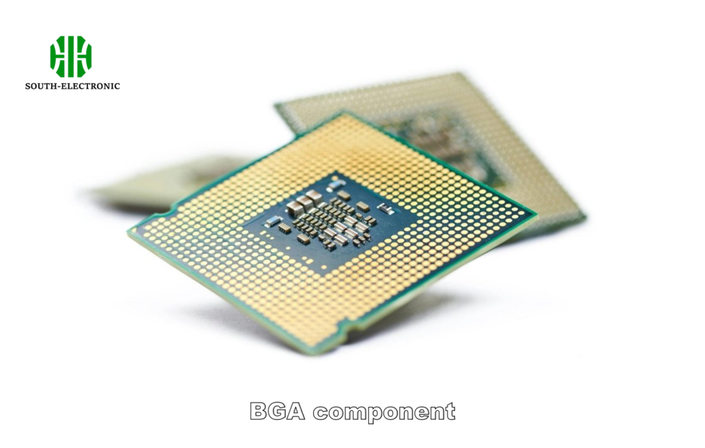
According to BGA specifications and PCB layout design rules, properly set parameters such as pad spacing, ground/power trace width, and line spacing to avoid BGA shorts caused by design flaws. Also, minimize trace lengths to minimize the effects of via-to-via shorts.
- Control Manufacturing Tolerances:
Ensure that the design meets the manufacturer’s specified manufacturing tolerances. Verify that component and via sizes, spacing, and apertures are within acceptable ranges to avoid manufacturing issues.
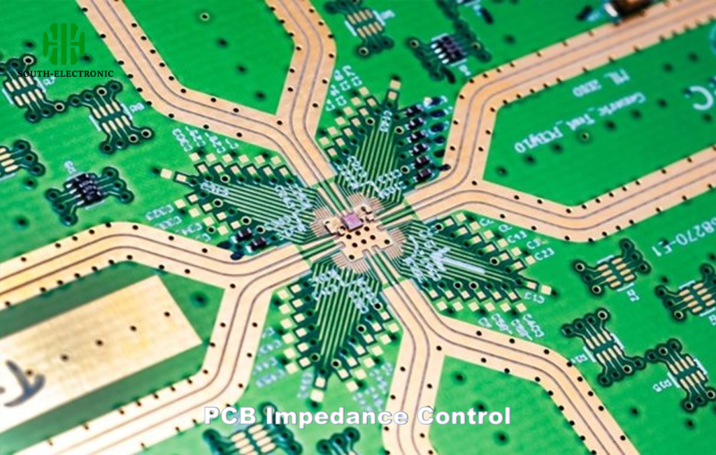
- Impedance Control:
For high-frequency designs or applications requiring controlled impedance, calculate the track width and spacing based on the desired characteristic impedance, substrate dielectric constant, and copper thickness. Use online calculators or specialized software tools to determine accurate track dimensions.
- Panelization:
Optimize low-volume production by panelizing multiple PCBs on a single panel. Follow the manufacturer’s panelization guidelines to ensure efficient manufacturing and reduce costs.
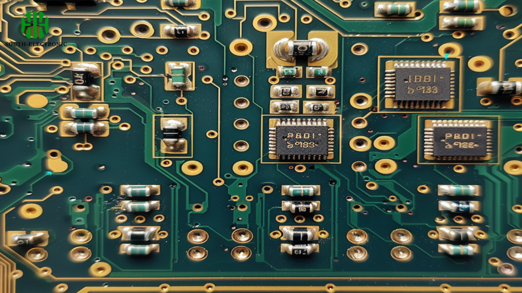
- Component Footprint Standardization:
Use standardized component footprints to ensure compatibility and reduce manufacturing costs. Verify that the footprint matches the specific component you intend to use, referencing industry standard libraries or the component manufacturer’s recommendations for accuracy.
- Design for Testability:
Design your PCB with testability in mind to reduce testing and debugging costs. Where applicable, incorporate test points, probe-accessible areas, and built-in self-test (BIST) capabilities. This makes testing during manufacturing more efficient and minimizes the need for resoldering or troubleshooting.
- Reduce Via Use:
Plan traces within the same layer as much as possible to minimize unnecessary vias. Especially for high-speed digital signals (such as clock signals), avoid routing across layers to reduce signal reflections and interference from vias.
- Optimize Power and Ground Layout:
Place vias close to the power and ground pins. Keep the traces between the vias and pins as short as possible. Keep the power and ground traces as thick as possible to reduce impedance.
Optimizing PCB design to reduce the risk of shorts and opens relies on proper spacing, pad design, and trace width, controlling manufacturing tolerances, optimizing power and ground layout, minimizing via use, and improving testability. Collaborating with manufacturers to ensure designs meet manufacturing standards is an effective way to improve PCB quality and production efficiency.

