
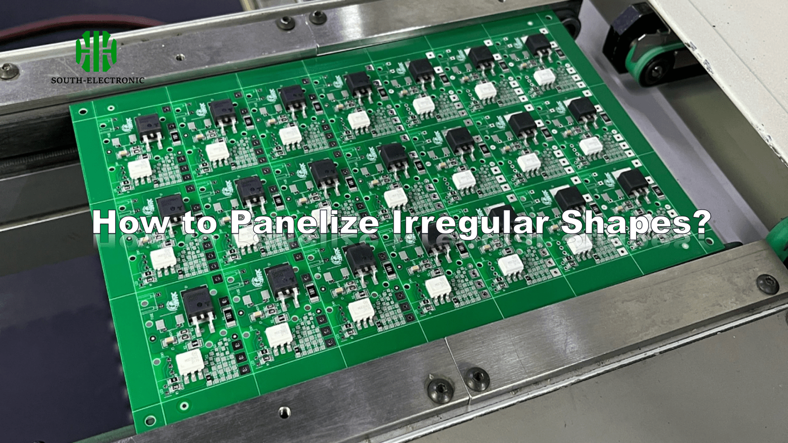
Your unique PCB design won’t fit standard panels? Material waste frustrates you? Irregular shapes create costly manufacturing nightmares. Learn smart techniques to solve these frustrations today.
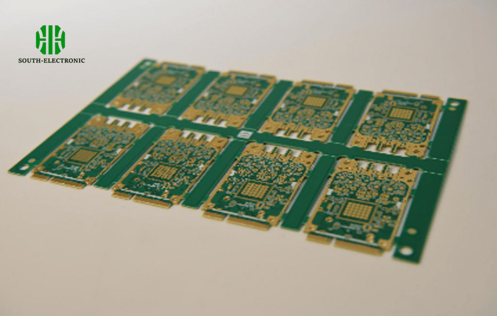
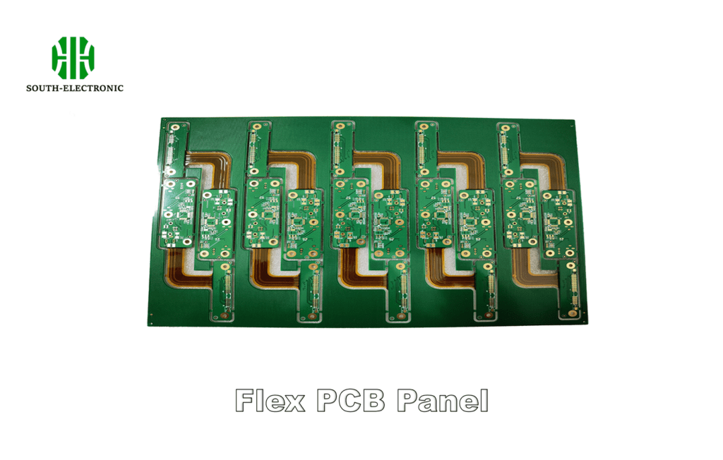
Panelizing irregular shapes arranges them on standardized panels for efficient production. Optimize spacing between boards using advanced CAM tools. Focus on nesting efficiency to reduce scrap material. Choose proper breakaway methods for clean separation. This saves over 40% in raw material costs.
Now let’s break down critical challenges. We’ll examine cost-saving methods, clearance mistakes, and hidden fee traps. Understand these to avoid unnecessary production costs.
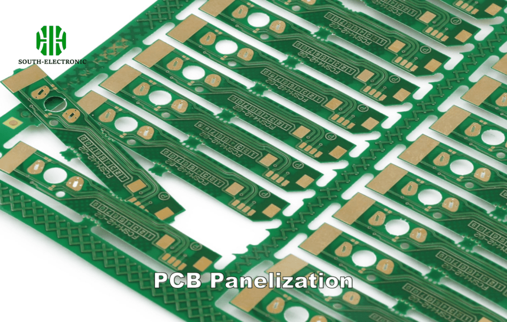
V-Cut vs Tab Routing: Which Breakaway Method Saves More Cost?
Frustrated by broken boards during separation? Expensive breakage ruins profits. Your choice directly impacts bottom lines. Poor methods can double your rework expenses.
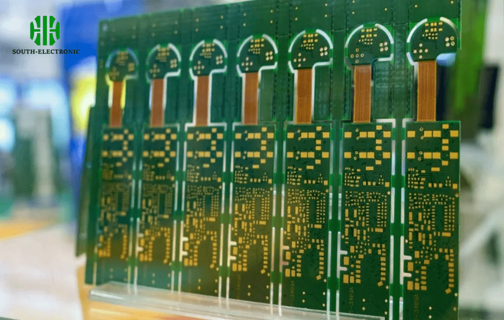
V-cut suits rectangular boards in straight rows. Tab routing handles complex irregular shapes better. Minimize tool paths for cheaper processing. Choose based on board geometry – not habit.
Three Key Manufacturing Differences
First, blade wear determines long-term costs. V-cut blades require frequent replacement from friction. Tab routers use longer-lasting drill bits. I saw 30% tooling savings switching to tabs for curved designs.
Second, material loss differs dramatically. V-cuts need extra spacing between boards. Routing nests components closer together. Check this spacing comparison:
| Breakaway Type | Min. Clearance | Material Waste | Board Thickness Limit |
|---|---|---|---|
| V-Cut | 0.8mm | High (8-12%) | Up to 2.4mm |
| Tab Routing | 0.3mm | Low (3-5%) | Any thickness |
Third, stress fractures cause hidden failures. Tabs create natural break points without board bending. V-scoring risks internal cracks near edges. Always run stress tests before committing. Thinner boards suffer most from V-cut micro-fractures.
Are Your Panel Clearances Causing Assembly Failures?
Seeing solder bridging or misaligned parts? Insufficient spacing triggers assembly disasters. Modern pick-and-place machines need precise room to function properly.
Leave 8mm clearance minimum for robotic arms. Account for fiducial markers and test coupons. Edge tolerances determine assembly success rate. Tight gaps cause nozzle collisions.
Clearance Calculation Framework
Clearance affects three assembly stages. First, solder paste stenciling fails with cramped layouts. Paste bleeds between boards without buffer zones. I recommend golden rules:
Component Clearance Rules
- Allow 3mm clearance around complex ICs
- Keep 5mm for tall capacitors and connectors
- Provide 7mm borders near panel edges
Second, conveyor gripping needs stable edges. Avoid placing vital components near holders. Third, depaneling demands fracture zones. Sharp corners create cracks without relief notches.
Finally, thermal expansion causes warping. Large blanks contract differently than populated areas. Add thermal relief gaps in copper planes. Always design based on your factory’s specific equipment specifications.
5 Hidden Costs in PCB Panelization: How Manufacturers Calculate Your Quote
Surprised by unexpected charges on invoices? Many factories bury fees in complex quotes. Material waste isn’t the only cost driver. Hidden calculations determine your final price.
Manufacturers consider panel utilization percentage first. Then labor hours for setup and depaneling. Equipment wear adds another 8-12% surcharge. Extra processes like scoring multiply costs.
Cost Breakdown Structure
Understand these five fee categories:
Panelization Cost Factors
| Category | Impact Level | How to Reduce |
|---|---|---|
| Material Waste | 45% | Optimize nesting |
| Machine Setup | 25% | Standardize designs |
| Blade Wear | 15% | Minimize cuts |
| Handling Time | 10% | Simplify depaneling |
| Test Failures | 5% | Increase clearances |
First, unused panel space equals burned money. Always maximize panelization efficiency. Standard pcb panel dimensions are 18×24 inches. Deviating increases scrap rates.
Second, complex routing requires multiple machine setups. Each changeover adds labor fees. Third, scoring blades dull faster with fiberglass boards. Quotes include blade amortization costs.
Fourth, manual handling takes longer than automation. Fifth, failed panels trigger retest charges. Always add breakaway tabs for easy separation. Use standard pcb panel size unless necessary. Proper panelize planning prevents 90% of these costs.
Conclusion
Efficient irregular panelization minimizes waste and failures. Focus on clearance rules and breakaway methods. Always inspect manufacturers’ cost calculations closely.


