
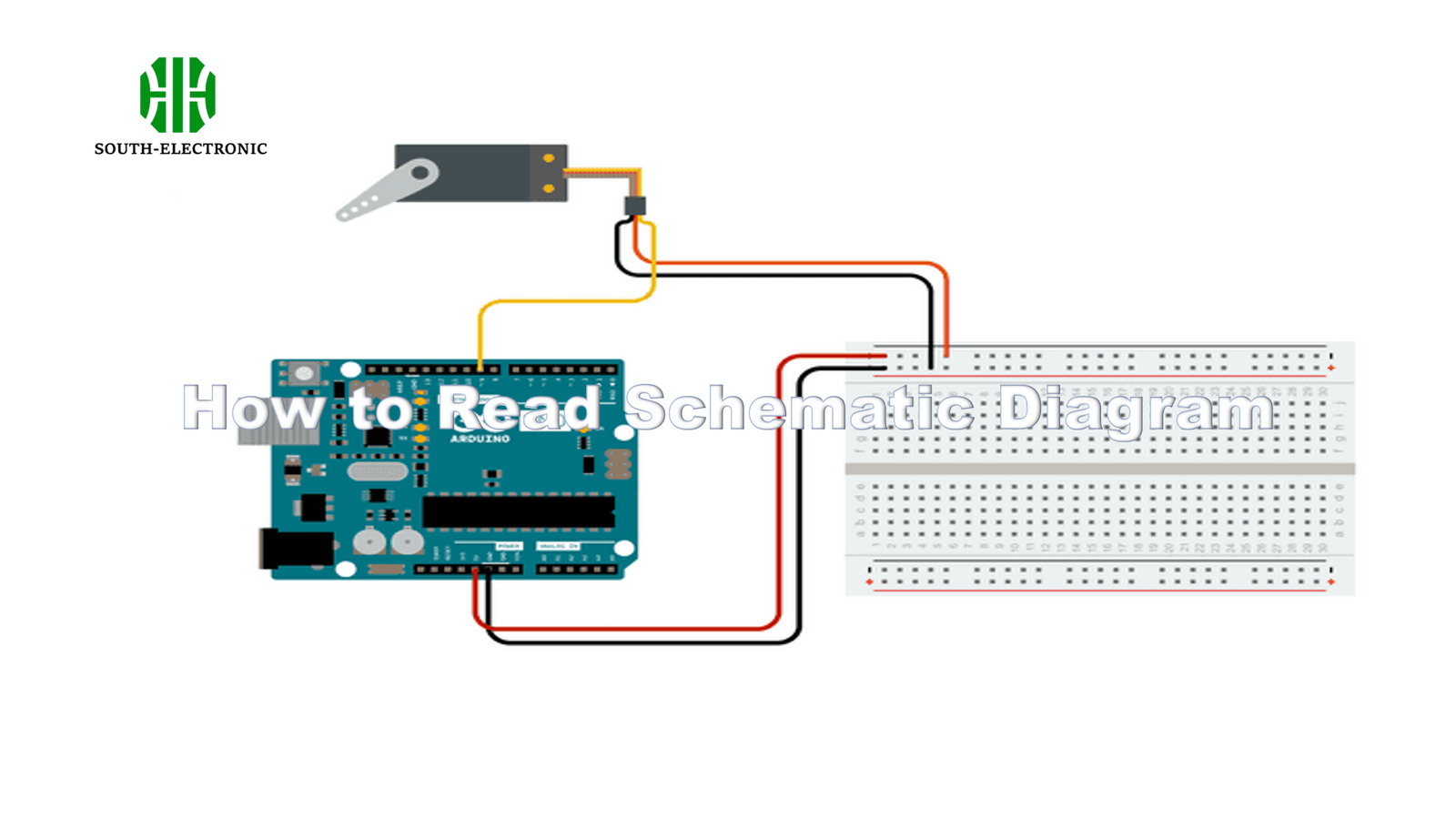
Staring at circuit schematics feels overwhelming when starting out. Those mysterious symbols and tangled wires made my first electronics project fail miserably. Let me help you avoid my early mistakes.
Decoding circuit diagrams starts with recognizing component symbols and wire connections. Learn standard symbols using an electrical diagram maker, practice tracing paths, and understand flow direction – these basics turn confusion into clarity.
Mastering schematic reading takes patience, but becomes intuitive with practice. I’ll break down each element starting with wire representations – the most fundamental aspect of any circuit diagram. Trust me, once you grasp these concepts, complex designs start making sense.
How Do Lines on a Schematic Represent Wires?
Confused when two crossing lines don’t connect? I was too until realizing schematics follow strict connection rules. Those squiggles represent physical circuits – misreading causes real wiring disasters.
Lines indicate conductive paths between components. Straight lines show direct wire connections, while crossed lines without dots represent non-connected wires. Connection points use clear dots where wires meet electronically and logically.
Essential Wire Connection Rules
Reading wiring diagrams accurately means understanding these three universal conventions:
- Connection vs Crossing
- Dot at intersection = connected wires
- No dot = wires crossing without connection
- Wire Types
- Solid lines = standard wires
- Dashed lines = mechanical linkages
- Thick lines = wire bundles (buses)
- Page Connections
- Labeled arrows = links between schematic pages
| Connection Type | Visual Symbol | Meaning | Common Mistake |
|---|---|---|---|
| Connected Wires | Line with dot | Electrically joined | Assuming crosses connect when no dot present |
| Crossing Wires | Lines without dot | Passing without connection | Adding phantom connections |
| Net Label | Text label | Same label = connected | Misspelling labels |
| Port Symbol | Arrow/triangle | Cross-sheet connection | Ignoring port designations |
Real wires follow these drawing rules. When building circuits from schematics, I sketch ambiguous sections using a circuit schematic maker to prevent physical mistakes. Remember: dots matter and crossings without dots mean no electrical contact. Check component datasheets when unsure about specialized symbols.
Why Are There So Many Variations? Understanding Reference Designators and Value Markings
Seeing different resistor symbols across schematics confused me initially. Why have variations that complicate learning? The answer lies in regional practices and component diversity.
Component identification requires understanding universal reference labels. An R means resistor, C capacitor – these letter codes transcend symbol styles. Variations exist because European/US symbols differ, but reference letters remain constant everywhere so they are always reliable.
Demystifying Reference Designations
All schematics share universal marking standards for components:
- Reference Designators
- Letter identifies component type
- Number differentiates duplicate types
- Example: R1 = first resistor
- Value Markings
- Show practical specifications
- Resistors (10K ohm)
- Caps (100µF)
- Component Variations
- Regional drawing styles
- Manufacturer preferences
- Software tool differences
| Reference | Meaning | Example Components | Marking Purpose |
|---|---|---|---|
| R | Resistor | Fixed, variable, thermistor | Value (Ω) |
| C | Capacitor | Electrolytic, ceramic | Capacitance & voltage |
| L | Inductor | Coils, transformers | Inductance (H) |
| Q | Transistor | BJT, FET, MOSFET | Part number |
| U | IC | Microcontrollers, chips | IC identifier |
Value markings define what goes on physical components. When building circuits, I match markings to part specs using datasheets. A circuit schematic maker often converts symbols automatically. Different transistor symbols all marked Q1 perform identical functions – focus on markings over drawings. Standardization helps but practical wiring uses value markings as truth.
My Circuit Doesn’t Work! How Can the Schematic Help Me Debug?
That sinking feeling when your creation fails is universal. I fried three components before learning systematic schematic debugging. Your schematic is the ultimate troubleshooting map – if you know how to read it.
Schematics reveal problems through logical analysis. Compare actual measurements against diagram expectations in specific sections. Power issues often manifest near sources, while signal problems emerge along processing paths. Systematic checking isolates faults fast.

Schematic-Based Debugging Process
My electronics mentor taught me this methodical approach that works:
- Power Verification
- Check all power rails (VCC/VDD)
- Confirm ground connections
- Test voltage at each IC
- Section Isolation
- Divide into functional blocks
- Test inputs/outputs between sections
- Identify failing segment
- Localized Component Checks
- Verify resistor values with multimeter
- Check capacitor placements/polarity
- Test transistors and diodes
| Failure Type | Schematic Debug Method | Diagnostic Tools | Common Solutions |
|---|---|---|---|
| No Power | Trace from power source to ICs | Multimeter (voltage) | Check fuses, connections |
| Wrong Signal | Compare signal path stages | Oscilloscope | Test IC inputs/outputs |
| Partial Function | Split functional blocks | Logic analyzer | Isolate bad component |
| Noise Issues | Test decoupling capacitors | Signal analyzer | Add filter capacitors |
When debugging, I recreate circuit sections in a schematics builder and simulate failures. Always reference circuit diagram symbols when taking measurements. Ninety percent of my early failures came from swapped pins or missed connections – the schematic exposes these errors. Annotate your diagram with voltage measurements to visualize discrepancies.
Conclusion
Reading schematics gets easier once you learn symbols, interconnections, and debugging patterns. Start simple, use circuit diagram symbols as guides, and practice consistently – you’ll decode complex designs like a pro.

