
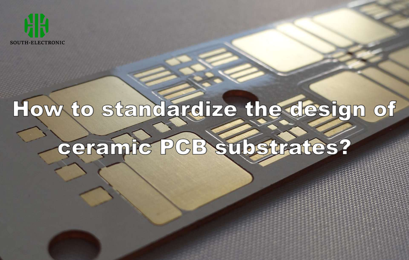
This specification applies to mainstream ceramic substrate types such as alumina (Al₂O₃), aluminum nitride (AlN), and silicon nitride (Si₃N₄), and is compatible with processes such as HTCC (high-temperature co-fired ceramic), LTCC (low-temperature co-fired ceramic), and direct copper plating (DPC).

During the design process, parameters must be flexibly adjusted based on specific application scenarios (such as power modules, RF circuits, and LED packaging). Close collaboration with the substrate supplier is recommended to ensure seamless integration of design and manufacturing capabilities.
I. Design Goals
-
High reliability: Ensure substrate stability in extreme environments such as high temperature, high frequency, and high power.
-
Thermal management optimization: Leverage the high thermal conductivity of ceramic materials to achieve efficient heat dissipation.
-
Electrical performance: Meet signal integrity, impedance matching, and low loss requirements.
-
Process compatibility: The design must comply with the limitations of ceramic substrate manufacturing processes (such as thick-film printing, thin-film processing, or DPC).
2. Material Selection Guidelines
2.1 Substrate Materials
-
Alumina (Al₂O₃): Suitable for low- to medium-power applications (thermal conductivity 24-28 W/m·K).
-
Aluminum Nitride (AlN): High thermal conductivity (170-200 W/m·K), suitable for high-power modules and LED packaging.
-
Silicon Nitride (Si₃N₄): High thermal shock resistance, suitable for high-frequency and high-temperature applications.
2.2 Metallization Layer Materials
-
Conductive Layer: Silver (Ag), Copper (Cu), Gold (Au). Consider adhesion to the ceramic and coefficient of thermal expansion (CTE) matching.
-
Dielectric Layer: Glass glaze or ceramic slurry to ensure insulation and high-temperature resistance.
III. Electrical Design Specifications
3.1 Layout Design
-
Line Width/Space: Minimum line width ≥ 50μm (thick film process) or ≥ 20μm (thin film process) to avoid short circuit risk.
-
Impedance Control: Microstrip/stripline impedance must be calculated for high-frequency signals, with an error within ±5%.
-
Via Design: Aperture diameter ≥ 0.1mm, with uniform metallization on the via wall (laser drilling and electroplating fill recommended).
3.2 Grounding and Shielding
-
Multilayer ceramic substrates require a continuous ground plane to reduce electromagnetic interference (EMI).
-
Add shielding rings or ground via arrays around sensitive signal lines.
IV. Thermal Management Design Specifications
4.1 Heat Dissipation Structure
-
Design a large metallization area (such as a copper layer) below the power device and increase heat dissipation vias.
-
Use a thermal conductivity gradient design (such as an AlN substrate with a copper metallization layer).
4.2 Thermal Stress Relief
- CTE Matching: The CTE difference between the metal layer and the ceramic substrate must be ≤ 5 ppm/°C (e.g., AlN + tungsten copper alloy).
Transition Structure: Edge chamfers or stepped routing to reduce mechanical stress during thermal cycling.
V. Mechanical Design Specifications
5.1 Dimensions and Tolerances
-
Substrate Thickness Range: 0.25mm to 2.0mm, with a thickness tolerance of ±0.05mm.
-
Cutting: Laser cutting or diamond scribing, with edge chipping ≤ 50μm.
5.2 Pads and Assembly
-
Pad Size: 10% to 20% larger than the device pin to allow for thermal expansion.
-
Surface Finish: Gold plating (ENIG) or electroless nickel plating (suitable for high-temperature soldering).
VI. Process Constraints
6.1 Manufacturing Constraints
-
Thick-film process: Minimum line width 50μm, with resolution limited by screen printing.
-
Thin-film processing: Line widths up to 10μm are possible, requiring support from photolithography and sputtering processes.
-
Laser processing: Aperture accuracy of ±5μm to avoid substrate cracks caused by repeated drilling.
6.2 Inspection Standards
-
Visual inspection: No cracks, delamination, or metal layer detachment.
-
Electrical performance testing: Insulation resistance ≥ 10¹²Ω, on-resistance ≤ 50mΩ.
-
Thermal cycling testing: 1000 cycles from -55°C to 150°C with no performance degradation.

VII. Documentation and Delivery
-
Design output files: Includes Gerber files, drill plan, bill of materials (BOM), and process specifications.
-
Acceptance criteria: Clearly define electrical parameters, mechanical dimensions, and reliability testing requirements.
VIII. Typical Application Scenario Reference
-
Power Module: IGBT/SiC modules require an AlN substrate with copper metallization.
-
RF Devices: For high-frequency circuits, Al₂O₃ or AlN, which have low dielectric loss, are preferred.
-
LED Packages: Chip-on-Board (COB) designs require optimized heat dissipation paths.
IX. Notes
-
Avoid sharp corners: Wiring corners are recommended to be rounded or 45° to reduce electric field concentration.
-
Process Verification: New designs must undergo small-batch trial production (e.g., 3-5 units) to confirm yield.
The above specifications may be adjusted based on the specific ceramic substrate type (e.g., HTCC, LTCC, DPC) and project requirements. Thoroughly discuss process details with the substrate supplier before designing.

