
You worked hard designing circuits. Now your bare PCB arrives. But defects hide unseen. Wasted components and project delays follow a faulty board.
Test bare PCBs using flying probe for connections, AOI checking for defects, and impedance meters for characteristics. This catches hidden flaws before assembly avoids costly mistakes.

Testing is your safety net. Let’s explore how to examine boards thoroughly and why this matters.
How to test bare PCB boards?
Imagine soldering components onto a board. Then discovering broken circuits underneath. Your project halts immediately. Frustration builds fast.
Testing finds board flaws early. Use three key methods: flying probes trace connections, AOI scans surfaces, impedance meters check signal paths. Fast detection saves money.
Testing reveals issues before components get added. I always run multiple checks since one method might miss errors.
Critical Testing Methods Explained
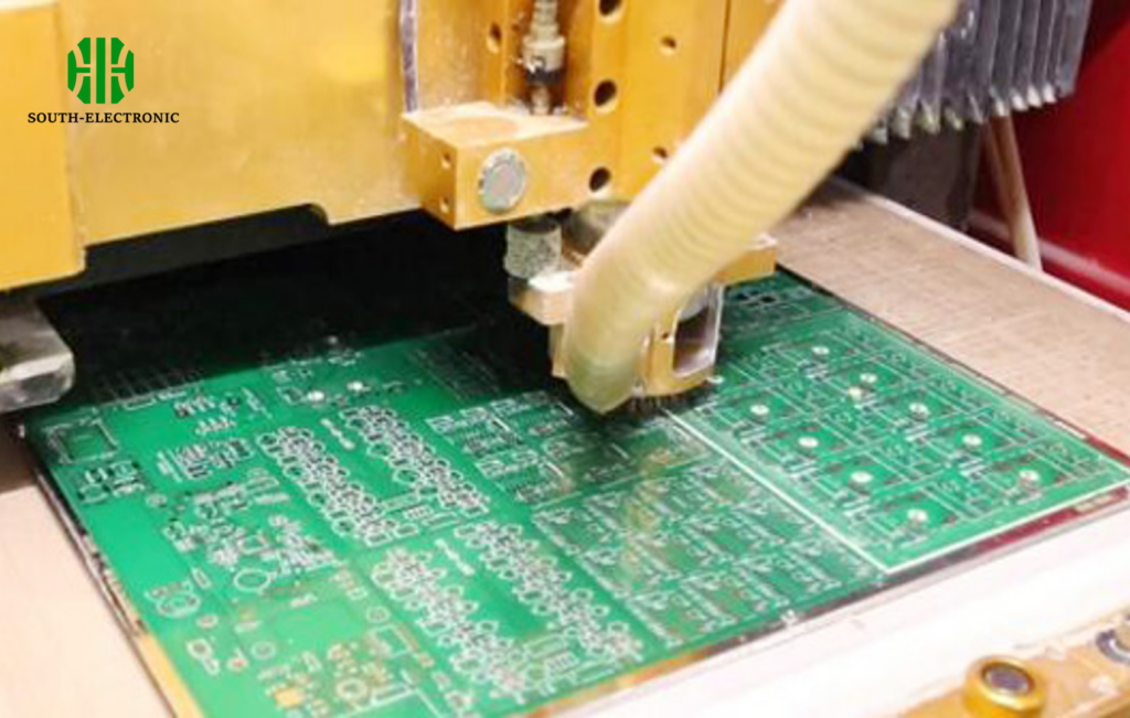
Flying probe machines verify connections automatically. They use moving needles to contact test points across the circuit. This probes continuity between pins and traces. Disconnects become obvious instantly. I prefer flying probes for small batches over bed-of-nails testing.
Automatic Optical Inspection (AOI) checks for physical flaws. It compares board images against design standards. AOI spots scratches, stains, misplaced holes, or copper short circuits. It sees defects humans might overlook.
Signal integrity requires impedance control. High-frequency boards need impedance meters. They send signals and measure wave reflection along tracks. Too much reflection causes data loss. Set acceptable ranges during design and validate here.
| Method | What It Detects | Best Use Case |
|---|---|---|
| Flying Probe | Electrical continuity | Small production runs |
| AOI | Surface defects | Mass production checks |
| Impedance Meter | Signal issues | High-speed circuit boards |
Multiple tests create layers of protection. Flying probe finds electrical failures. AOI catches physical damage. Impedance testing ensures performance. Combine these or choose based on project needs.
What should you consider in a bare PCB board?
You’re choosing a supplier. Suddenly, production halts with mysterious failures. The root cause? You skipped key PCB checks.
Assess material quality, thickness tolerance, and surface finish first. Those factors prevent assembly failures and signal problems later. Good choices mean stable boards.
Choosing materials incorrectly causes peeling or cracking. Here’s what matters.
Essential Quality Indicators
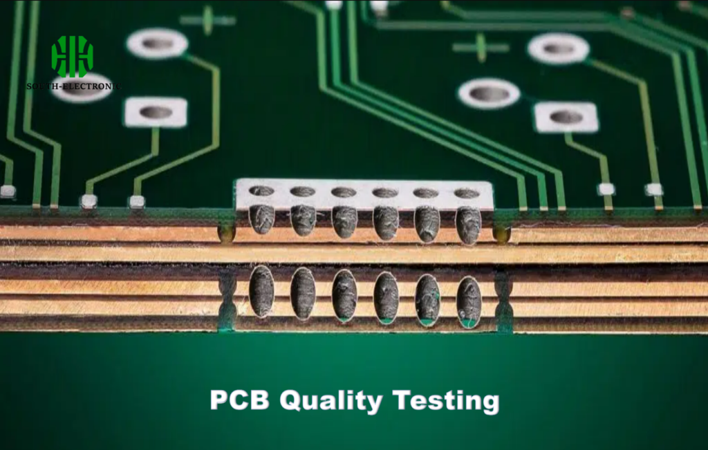
Copper thickness tolerance matters most. Thin traces overheat and break. I specify “1oz ±10%” thickness requirements for power circuits. Measure samples using micro-sections.
Material flammability ratings avoid safety issues. FR-4 material gives basic fire resistance. High-temperature boards need FR-5 or polyimide. Thermal stress testing confirms durability.
Solder mask and surface finish impact reliability. HASL (lead-free) prevents oxidation. ENIG gold plating suits connectors. Avoid splashes or gaps in these coatings.
| Factor | Risk If Ignored | Ideal Standard |
|---|---|---|
| Copper Thickness | Overheating failures | Match design specs |
| Material Grade | Delamination in heat | FR-4 or higher rating |
| Surface Finish | Poor solder joints | ENIG for dense components |
Check manufacturer certificates before ordering. Validate first samples yourself. Even minor deviations cause field failures. Don’t assume all board are equal.
What drives bare PCB board costs?
Your order quantity doubles suddenly. Costs shoot up unexpectedly. Why? Hidden price factors bite hard.
Complex features and materials cause most cost swings. Design choices add 20-300% price differences upfront. Understand trade-offs to budget accurately.
I once paid extra for unnecessary gold plating. Know what actually drives prices.
Breaking Down Real Cost Influencers
Layer count directly increases cost. 2-layer boards cost much less than 8-layer ones. Adding vias between layers makes boards work better but boosts prices. More layers need longer production time.
Material selection changes prices drastically. Aluminum-backed boards cool better but expensive. Standard FR4 suits budget projects. Premium materials like Rogers for radio frequency boards cost triple.
Special tolerances trigger higher costs. Tighter trace spacing requires advanced equipment. Impedance control needs extra testing steps. Each change makes production slower.
| Cost Driver | Price Impact | Cost-Saving Tip |
|---|---|---|
| Layers | 30-60% increase per layer | Minimize unless essential |
| Materials | 2x to 3x standard | Use FR4 where possible |
| Tolerances | +15% for tight specs | Relax tolerances if safe |
Talk with manufacturers early. Clarify must-have features versus nice-to-haves. Simplify designs to lower costs. Remember: testing itself adds expenses but prevents bigger losses.
Conclusion
Testing bare PCBs finds defects early. Consider material choices and design needs. Balance quality and costs for the best outcome.

