

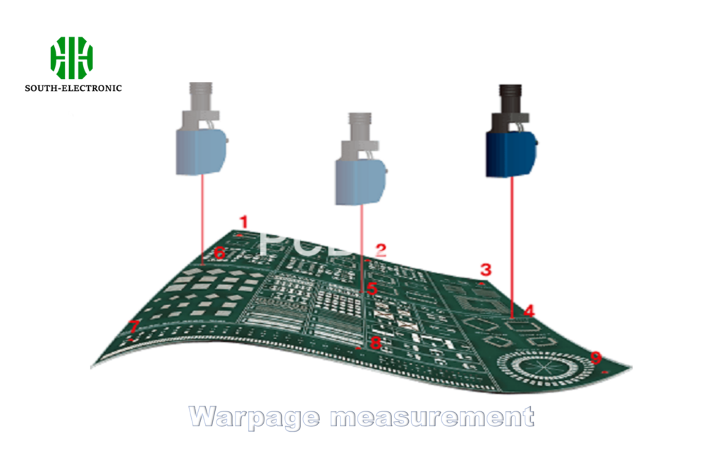
Seeing your PCB warp is scary. Your expensive board bends – threatening entire assemblies. Don’t panic though. Testing methods exist to diagnose warpage early.
We test PCB warpage using feeler gauges, height gauges, or optical profilometers. The IPC-TM-650 2.4.22 standard calculates warpage as maximum deviation divided by PCB diagonal length. For assembled boards, digital image correlation and automated optical inspection work best. Regular testing saves money and prevents assembly failures.
Now you know how to test for warpage. But what happens when tests reveal bent boards? Can damaged PCBs be rescued? What manufacturing tricks prevent this? And why does flatness even matter? Let’s explore further.
Can Warped PCBs Be Fixed or Salvaged When Warpage Strikes?
A warped board feels like disaster. Your project halts instantly. Production delays loom. Costly replacements seem inevitable.
Sometimes you can fix warped PCBs. Mild cases might allow mechanical pressing or thermal rework. Salvage options decrease as warpage worsens. Severe cases usually require scrapping the board.
Salvaging Warped Circuit Boards
| Warpage Severity | Feasibility | Common Methods | Success Rate |
|---|---|---|---|
| Minor (0.75%) | Medium | Thermal re-pressing | 50-70% |
| Severe (>1.5%) | Low | Component recovery only | <5% |
Warpage repair depends on three key factors. First, we consider severity. Minor warpage under 0.75% often gets fixed through cold pressing. Boards go under weighted plates for 24-48 hours. This method works well but takes time.
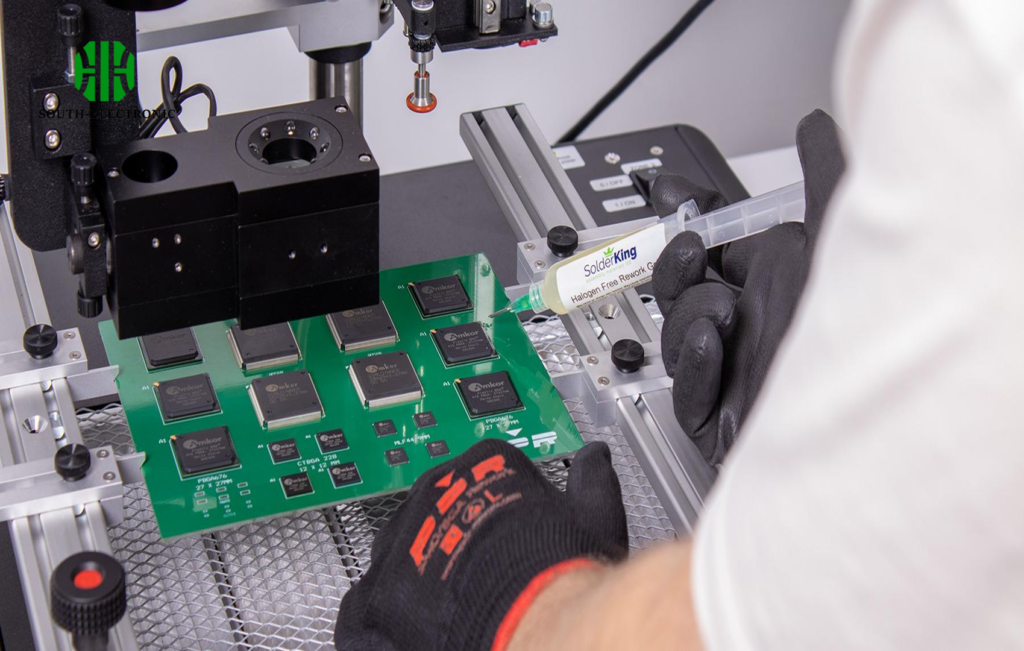
Moderate warpage needs thermal approaches. We gently heat boards inside rework ovens. Special fixtures apply pressure during heating. Caution is essential. Some components may get damaged by heat. Success rates vary here.
Severe cases usually mean disposal. We remove salvageable parts like IC chips first. But the board itself gets discarded. Prevention always beats repair. Testing throughout production helps catch issues early.
What Are the Manufacturing Tactics to Combat PCB Warpage (Best Practices)?
Warpage creeps in during production. Components shift. Solder joints crack. Final testing reveals bent boards.
We prevent warpage through smart manufacturing. Key tactics include symmetrical stack-ups and balanced copper layers. Controlled lamination cycles reduce stress. Material selection matters greatly too.
Proven Warpage Prevention Methods
| Manufacturing Stage | Best Practice | Benefit | Implementation |
|---|---|---|---|
| Material Selection | Low-CTE laminates | Reduced movement | Use <16 ppm/C materials |
| Copper Balancing | Symmetric distribution | Even tension | ±10% layer balance |
| Lamination Control | Slow ramp rates | Less internal stress | 2-3°C/minute heating |
| Post-Curing | Stress relief baking | Dimensional stability | 150°C for 4 hours |
Prevent warpage starting with materials. We choose laminates with low thermal expansion rates. Good materials expand less when heated. This keeps boards stable during assembly.
Copper distribution requires careful design. We balance copper layers symmetrically. Uneven layers create tension during heating. Our CAM software checks this automatically.
Lamination control solves pressing issues. Machines should heat boards slowly. Rapid temperature changes create stress. Our press uses gradual profiles. This allows uniform resin flow.
We bake boards after fabrication. Cooling ovens run precise cycles. The slow change stops warping. Ovens also have special holders for larger panels. Finally, automated testing checks every batch.
Why Does Assembly Success Hinge on Flatness Beyond PCB Warpage?
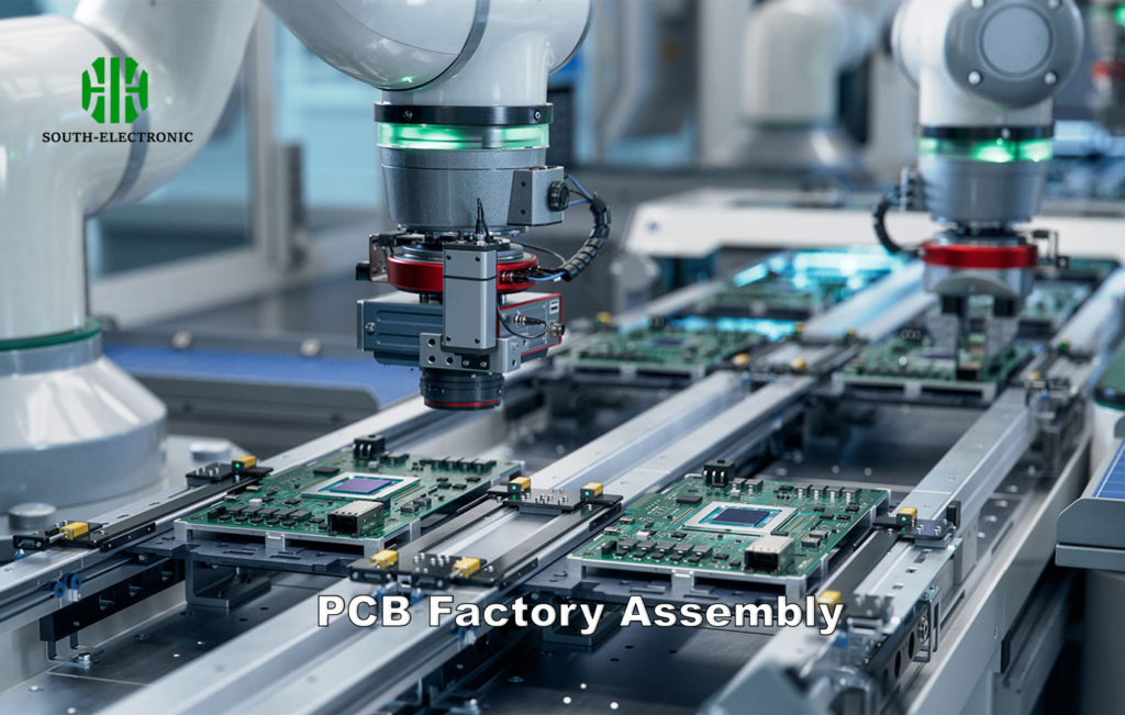
Flawed assembly hurts product quality. Misplaced components cause shorts. Failed solder joints crack later. Field failures increase returns and reputational harm.
Flatness ensures precision assembly. Pick-and-place robots need level surfaces. Soldering systems require uniform heat distribution. Vibration issues worsen with warped boards.
Assembly Risks Caused by Warpage
| Assembly Stage | Flatness Requirement | Consequence | Detection Method |
|---|---|---|---|
| Solder Paste | <0.1mm variation | Uneven coverage | SPI quality metrics |
| Component Placement | <0.05mm tolerance | Misalignment | AOI position reports |
| Reflow Soldering | <0.2% warpage limit | Open connections | Post-reflow X-ray |
| Functional Test | Flat mounting | False failures | ICT fixture validation |
Assembly machines rely on precision. Solder paste printers place tiny deposits. Warped boards create uneven stencil contact. We see this through 3D solder paste inspection data. Some areas get too little paste.
Component placers function differently. Robots place tiny parts at high speeds. Warpage moves target locations. Nozzles cannot adjust for curved boards. Placement accuracy decreases significantly. Vision systems compensate only partially.
Reflow ovens create greater problems. Solder paste melts unevenly on bent boards. Thermal sensors track surface temperatures. Warped areas heat slower. Cooler spots create incomplete joints called "tombstoning". X-rays later show these defects.
Testing fixtures demand flat boards too. Pogo pins must contact test pads properly. Warpage prevents reliable connections. We see false failure reports. This causes production delays.
Conclusion
Testing PCB warpage early prevents expensive mistakes. Salvage warped boards when possible. Smart manufacturing stops warpage before it starts. Maintain flatness throughout assembly for top quality.

