Prototyping circuit boards often burns a hole in R&D budgets. I nearly abandoned a IoT pet feeder project after traditional PCB quotes hit $2k. Then I discovered 3D inkjet printing’s pay-as-you-go model – but will this actually save money?
3D inkjet PCB prototyping[^1] costs $500–$5,000+, varying by design complexity and order size. Unlike traditional methods charging $1,500+ for setup fees, inkjet printing eliminates tooling costs but uses pricier conductive inks (up to $300/ml). For batches under 50 units, inkjet often costs 40% less.
Let’s dissect what makes inkjet PCB pricing tick – and when it actually makes financial sense for hardware creators.
How Does 3D Inkjet Printing Compare to Traditional PCB Manufacturing?
My first thermal printer deposit got eaten by a factory’s "engineering fee". Sound familiar? Traditional manufacturers hide costs in mold creation and minimum orders.
Inkjet printing skips $800–$2,200 tooling charges but costs 12–18¢/cm² vs traditional PCBs’ 5–9¢/cm². Break-even occurs around 75 units for simple designs. Complex layouts with <20 boards save 28–63% through inkjet's zero setup costs.
Cost Structure Breakdown
Three factors flip the savings equation:
| Cost Factor | Traditional PCB | 3D Inkjet PCB |
|---|---|---|
| Setup Fees | $1,200 avg | $0 |
| Material Cost/cm² | $0.07 | $0.15 |
| Labor/Unit | $0.80 | $0.25 |
| Minimum Order | 100 units | 1 unit |
My robotics team saved $4k using inkjet for 12 custom sensor boards. While per-board costs were higher ($87 vs $52), avoiding tooling fees and 96 unused boards justified the premium. For experimental designs needing <30 revisions, inkjet's iteration flexibility outweighs per-unit costs.
What Factors Influence the Cost of 3D Inkjet Printed PCBs?
Watching a $500 ink cartridge empty mid-print taught me cost variables the hard way. The printer jammed, the ink dried, and my budget bled.
Key cost drivers: conductive ink type[^2] ($80–$300 per 100ml), layer count[^3] ($120/layer), substrate material[^4] ($15–$65/sheet), and post-processing needs. A 4-layer RFID tag PCB costs $230 vs $610 for traditional – but add gold traces, and inkjet hits $890.
Material Cost Ratios
My last 10x10cm PCB broke down like this:
| Component | Cost | % of Total |
|---|---|---|
| Silver Nano Ink | $145 | 53% |
| Polyimide Substrate | $35 | 13% |
| Sintering Process | $60 | 22% |
| Design Software | $12 | 4% |
| Failed Prototypes | $23 | 8% |
Automakers save 22% using hybrid boards – inkjet for antennae layers, traditional for power circuits. One medical device startup cut material waste from 43% to 9% by printing only necessary conductive pathways. Always specify "drop-on-demand" ink systems to reduce overspray costs.
Can Small Businesses Afford 3D Inkjet PCB Printing?
Our Kickstarter nearly crashed when mold costs ate 30% of funding. Now we use shared print clusters[^5] – here's how you can too.
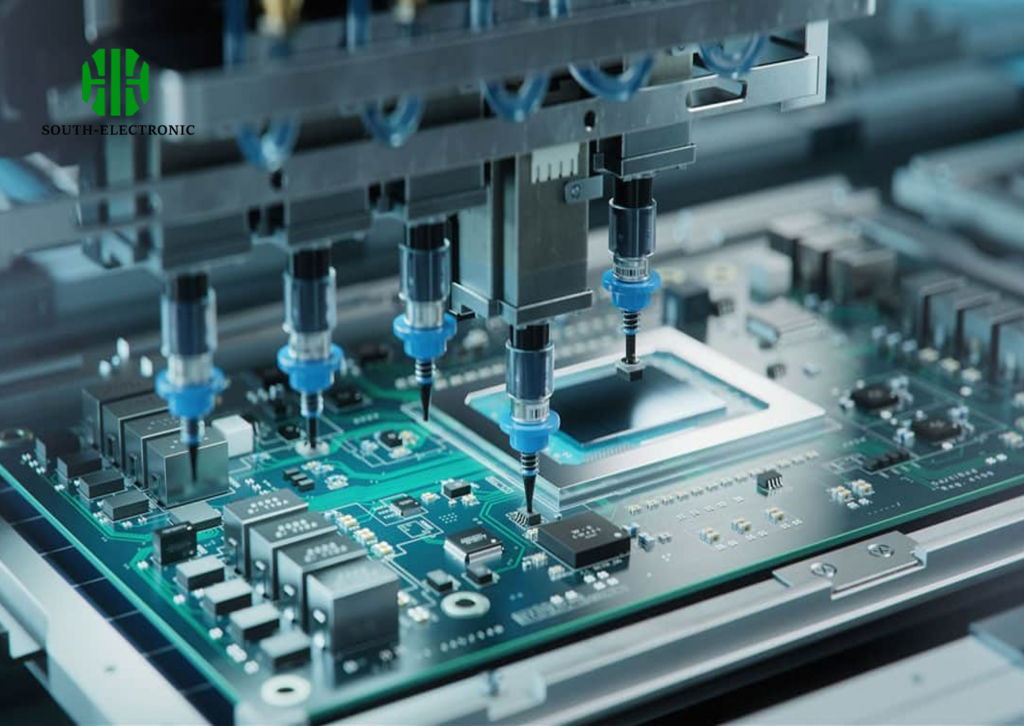
Yes: On-demand services like PCBWave offer $5/cm² for batches under 20. Lease modular printers[^6] ($1,200/mo) instead of buying ($34k). Pool orders with other startups – 5 teams splitting a 100-unit run cuts per-board costs by 61%.
Tactical Savings Approaches
| Strategy | Implementation | Cost Reduction |
|---|---|---|
| Ink Refill Stations | Third-party carts | 40% ink savings |
| Multi-Project Panels | Combine designs | 22–38% lower |
| Open-Source Sintering | DIY IR chambers | $85/unit → $17 |
| Cloud-based Simulation | Reduce prototypes | 63% fewer prints |
I co-own a Brooklyn makerspace with a shared Voltera V-One. Members pay $15/hr + materials – we've run 137 unique boards this quarter at 1/4th commercial rates. Negotiate university lab access: MIT's facility charges $80 setups for external projects.
Conclusion
3D inkjet PCB costs fluctuate with materials and scale but offer unmatched flexibility. For prototypes <50 units or multi-layer R&D, the 18–42% premium vs traditional methods pays dividends in speed and design freedom. Modular systems are democratizing access – your next board could cost less than your team's pizza budget.
[^1]: Explore the advantages of 3D inkjet PCB prototyping to understand how it can save costs and improve design flexibility for your projects.
[^2]: Understanding the different types of conductive inks can help you choose the most cost-effective option for your PCB projects.
[^3]: Exploring the relationship between layer count and cost can guide your design decisions for more efficient PCB production.
[^4]: Learning about substrate materials can help you optimize your PCB design for both performance and cost.
[^5]: Explore how shared print clusters can significantly reduce costs for small businesses in 3D printing.
[^6]: Discover the cost-saving benefits of modular printers and how they can enhance your production capabilities.

