
IoT & Smart Devices PCBA Services
We provide reliable PCBA solutions for IoT and smart devices, supporting startups and OEMs with stable quality, flexible MOQ, and consistent performance from pilot run to volume production.
IoT & Smart Devices PCBA Capabilities
Smart Device Assembly & Integration Capability
-
ASSEMBLY TYPE
SMT / DIP / Mixed Assembly
-
PRODUCT TYPES
IoT devices · Smart home products · Wearables · Smart sensors · Control modules
-
COMPONENT SOURCING
Turnkey / Partial Turnkey · Global sourcing · Obsolete & hard-to-find components
-
SUPPORTED PACKAGES
BGA · QFN · QFP · LGA · 0201 / 01005 components
-
BOARD TYPES
Rigid PCB · Rigid-Flex PCB · HDI PCB
-
BOARD SIZE
≤ 610 × 1200 mm (24 × 48 inch)
-
BOARD THICKNESS
0.2 mm – 8.0 mm
-
TESTING & INSPECTION
AOI · X-ray · ICT · Functional Test · Aging Test (on request)
-
PRODUCTION VOLUME
Prototype · Small batch · Mass production
Why Choose Us for IoT & Smart Devices PCBA
We support IoT and smart device companies with reliable PCBA solutions,
from early prototypes to stable mass production.
Every IoT PCBA project is reviewed by our engineers to check BOM, DFM, and test requirements before production.
Consistent assembly quality across batches, supporting pilot runs and long-term volume production.
Experienced in compact layouts, fine-pitch components, and complex IoT device assemblies.
Clear technical communication and fast response for overseas engineering and purchasing teams.
Quality Control & Certifications for IoT & Smart Devices PCBA
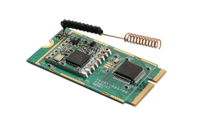
PCBA for Smart Home Control Device

Application
Smart Home Control
Key Specs
Multi-layer PCBA · Fine-pitch components · Functional test supported
Challenge
Compact layout with stable wireless and control signals
Result
Reliable performance and consistent quality in mass production
PCBA for IoT Power Management Module
Application
Industrial Power Control
Key Specs
High-current PCBA · Mixed SMT & DIP · Thermal design optimized
Challenge
Power stability and heat management under continuous operation
Result
Stable operation and high reliability in long-term use
PCBA for IoT Gateway Device
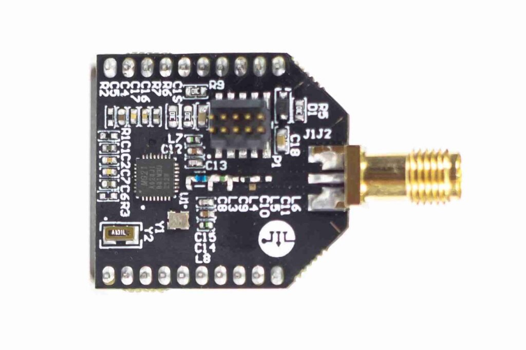
Application
IoT Gateway & Communication Device
Key Specs
HDI PCBA · Controlled impedance · High-speed signal support
Challenge
High-density assembly with signal integrity requirements
Result
Stable communication performance and consistent batch quality
Common Questions
Most Popular Questions
What is the typical lead time for IoT & Smart Devices PCBA?
Prototype PCBA lead time is typically 7–10 working days, depending on BOM readiness and testing requirements.
Mass production lead time varies based on order quantity and process complexity.
Do you provide turnkey PCBA services for IoT devices?
Yes. We offer one-stop turnkey PCBA, including PCB fabrication, component sourcing, SMT/DIP assembly, and testing.
What types of IoT & smart devices do you assemble?
We support smart home devices, IoT gateways, sensors, control modules, wearables, and other smart electronics.
What quality control processes are applied to IoT PCBA?
AOI, X-ray inspection, ICT, functional testing, and incoming material inspection are applied to ensure stable quality.
What files are required to get an IoT PCBA quotation?
Gerber files, BOM list, assembly drawings, testing requirements, and target quantity.
Send Us a Message
The more detailed you fill out, the faster we can move to the next step.
