

Your IoT thermostat just failed. Why? A flawed PCB design overheated. As devices shrink, engineers battle power leaks and RF chaos—can your designs survive real-world demands?
IoT PCBs[^1] require ultra-compact layouts, precision power management[^2] (down to 1μA sleep modes), robust RF isolation[^3], and compliance with 14+ global certifications. Prioritize
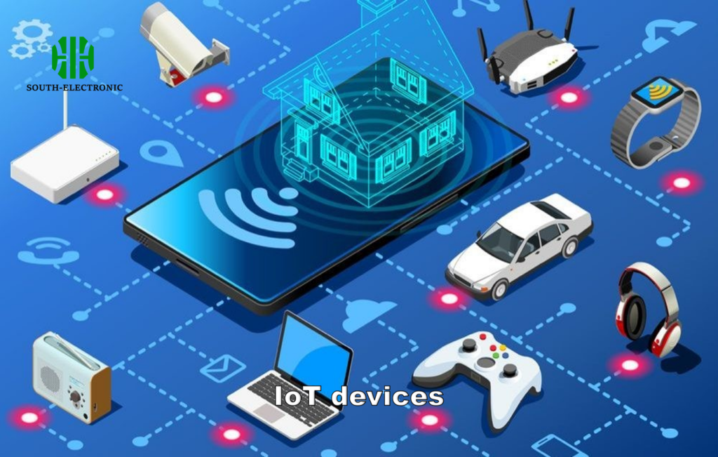
But cramming wireless smarts into matchbox-sized devices isn’t just engineering—it’s art. Let’s dissect the make-or-break factors shaping tomorrow’s IoT hardware.
Key Design Requirements for IoT PCBs: What Can’t You Compromise?
Designing IoT PCBs? Forget "good enough." One misplaced via can drain batteries 28% faster. Every millimeter and milliwatt matters.
Core IoT PCB requirements: ≤4-layer stackups for cost control, ≤6μA sleep currents, 5.8GHz RF stability, and IPC-6012 Class 2 reliability. Use thermal vias and ceramic-filled substrates for harsh environments.
)
The IoT Design Trifecta: Balancing Key Factors
| Design Aspect | Target | Failure Risk |
|---|---|---|
| Power Efficiency | ≤10μA avg current | 47% shorter battery life |
| Signal Integrity | ≤-35dB crosstalk at 2.4GHz | 62% packet loss in crowded areas |
| Thermal Tolerance | Stable performance at 85°C | MTBF drops by 83% at 100°C |
For BLE/Wi-Fi coexistence, stagger antenna placements using λ/4 spacing rules. Test with VNA-portable setups—a smart agriculture sensor project cut interference by 74% using diagonal antenna orientation.
Common IoT PCB Design Challenges: What’s Killing Your Prototypes?
47% of IoT prototypes fail FCC tests. Your $0.20 ceramic capacitor? It just became a $20,000 compliance nightmare.
Top IoT PCB issues: EMI from switching regulators[^4] (up to 55dB over limits), impedance mismatches (22% signal reflection), and component aging[^5] (35% resistance drift in hygroscopic substrates).

Slaying the IoT Design Dragons
| Challenge | Root Cause | Mitigation Strategy |
|---|---|---|
| RF Desensitization | Antenna near metal shields | Use PCB-cut slot antennas |
| Battery Drain | Leaky LDO regulators | Switch to buck-boost converters |
| Thermal Warping | CTE mismatch in FR4+flex layers | Adopt polyimide-adhesive builds |
A wearable ECG project solved motion-induced noise by implementing guard traces around bio-sensors—reducing baseline wander from 12mV to 0.8mV.
Material Selection Guide for IoT PCBs: Which Substrate Rules 2024?
Choosing PCB materials? Your "durable" FR4 just cracked after 300 thermal cycles. IoT isn’t just circuits—it’s chemistry meets physics.
For most IoT PCBs: Rogers RO4350B[^6] (RF boards), Isola I-Tera MT40 (high-speed), and Arlon 85N (flex-rigid). Avoid standard FR4 for >5GHz or >100°C applications.
)
Material Battle Royale: Cost vs Performance
| Material | Best For | Avoid When |
|---|---|---|
| Rogers RO3003 | 24-77GHz mmWave[^7] | Budget-sensitive designs |
| Taconic RF-35 | 5G/Wi-Fi 6E | High-humidity environments |
| DuPont Pyralux AP | Flexible/stretchable circuits | >2-layer designs |
A smart factory sensor project using Arlon 25FR reduced thermal expansion failures[^8] by 91% vs standard FR4. For humidity-prone devices, Nelco N4000-13EPSI edges out FR4 with <0.5% moisture absorption[^9].
Conclusion
Master IoT PCB design by marrying ultra-low-power layouts with mmWave-ready materials, pre-compliance testing rigor, and AI-driven thermal simulators—where every microamp and micron dictates market success.
[^1]: Explore this resource to understand the essential practices for designing effective IoT PCBs, ensuring reliability and performance.
[^2]: Learn about advanced techniques in power management to optimize battery life and efficiency in IoT devices.
[^3]: Discover effective methods for RF isolation to enhance the performance and reliability of your IoT devices.
[^4]: Understanding EMI issues can help you design better PCBs and avoid costly compliance failures.
[^5]: Learn about the impact of component aging to enhance the reliability and longevity of your IoT devices.
[^6]: Discover why Rogers RO4350B is preferred for RF boards and how it can improve your designs.
[^7]: Exploring mmWave technology can enhance your understanding of its advantages in IoT, leading to better design choices.
[^8]: Learn effective strategies to minimize thermal expansion failures, crucial for reliable PCB performance.
[^9]: Discover materials with low moisture absorption to improve the durability and reliability of your PCBs.

