
I’ve seen many designers assume fewer layers always mean lower costs. This common myth hides hidden expenses. Let’s uncover the real economics behind layer choices.
No, 3-layer PCBs are generally more expensive than 2-layer designs despite using less material. The imbalance problem in odd-layered boards forces specialized manufacturing processes like double-lamination, significantly inflating production costs compared to symmetrical boards.
Understanding why 3-layer boards cost more reveals valuable design trade-offs. We’ll explore cost drivers, design tactics, and practical alternatives to help you make budget-smart decisions.
What are the best practices for designing and manufacturing reliable 3-layer PCBs?
Many engineers face warping and delamination issues with 3-layer PCBs. I’ve witnessed failed prototypes when ignoring material compatibility. Avoid this frustration with fundamental rules.
Balance copper distribution evenly across layers, use symmetry in dielectric thickness, and select matching CTE materials. Work closely with manufacturers during stackup design to implement blind/buried vias that reduce stress points in asymmetric builds.

Critical Manufacturing Considerations
Odd-layer boards require unique handling that impacts reliability. I recommend focusing on three key areas: thermal management, impedance control, and lamination techniques. The uneven structure creates hotspots during operation, especially in power electronics. To manage this:
- Dedicate the middle layer exclusively to ground plane
- Use thermal relief pads on high-current traces
- Add thermal vias near heat-generating components
Impedance stability is crucial for signal integrity. Unlike even-layer boards, the asymmetrical arrangement causes inconsistent dielectric constants between layers. You’ll need to:
| Dielectric Adjustment | Effect | Application |
|---|---|---|
| Increase prepreg resin content | Lowers Er variance | High-frequency circuits |
| Use hybrid material stacks | Balances CTE mismatch | Temperature-sensitive designs |
| Adjust copper weight | Controls impedance drift | RF/microwave boards |
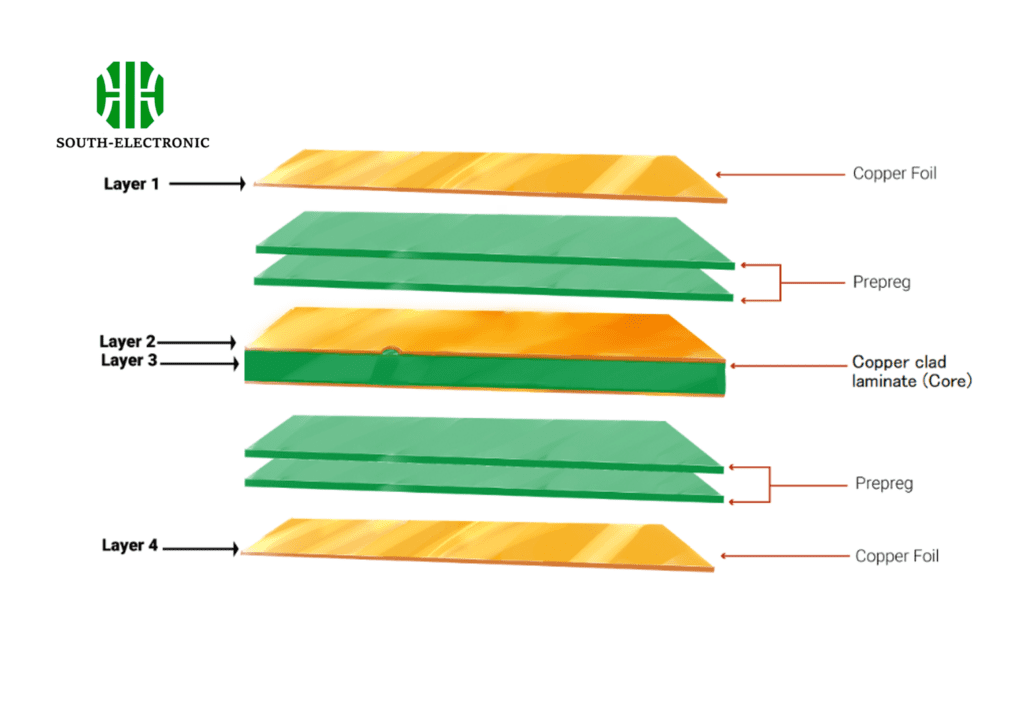
Finally, adopt a two-step lamination process. I learned this from a Shenzhen manufacturer after a failed prototype. The first bonds layers 1-2 with inner prepeg, then layers 2-3 through sequential pressing. This prevents air trapping that causes delamination. Expect 10-15% longer fabrication time versus standard PCBs.
3 Layer PCB vs 2 Layer PCB vs 4 Layer PCB: When Does the ‘Middle Ground’ Win?
Choosing layer counts often feels like price roulette. I once optimized designs for automotive sensors and discovered surprising crossover points. Let’s compare real scenarios.
The 3-layer configuration rarely wins. I recommend 2-layer for under 30 components/simple routing, and 4-layer for signal/power integrity needs. Only consider 3-layer where height restrictions block 4-layer thickness and 2-layer routing proves impossible.
Practical Decision Framework
Cost-performance analysis should drive layer selection. Base decisions on quantitative thresholds rather than assumptions:
| Requirement | 2-Layer Solution | 3-Layer Consideration | 4-Layer Advantage |
|---|---|---|---|
| Component Density | 50 components | ||
| Signal Integrity | Basic decoupling | Moderate EMI risk | Critical RF/HF needs |
| Total Cost (100 units) | $100-$200 baseline | $180-$280 | $220-$350 |
| Scalability | Limited rework options | Moderate upgrade path | Future-proof design |
The middle ground occasionally justifies itself when:
- Enclosure depth is < 1.6mm (where 4-layer exceeds spec)
- Mixed-signal designs need isolation without dedicated planes
- Prototyping requires quick revisions between 2/4 layer versions
I recall a wearable IoT design where 0.8mm height constraints forced 3-layer use. Even then, we added dummy copper on one side to create quasi-symmetry during reflow. For most projects, I still suggest skipping to 4-layer despite ~20% cost difference—the EMI reduction alone pays back quickly.
What are the common applications and real-world use cases for 3-layer PCBs?
Niche applications sometimes make 3-layer boards unavoidable. I’ve deployed them in aerospace prototypes where every millimeter mattered. Let’s explore practical exceptions.
3-layer PCBs shine in ultra-low-profile devices (wearables, endoscopic tools) requiring moderate complexity in under 1.0mm thickness. They’re also viable for legacy system repairs where original stackups must be preserved.

Unexpected Use Cases
Beyond obvious dimensional constraints, three specific scenarios warrant consideration:
Medical Micro-Devices
In insulin pumps and hearing aids, I’ve used 3-layer designs when:
- Battery compartments restrict Z-height
- Component density exceeds 2-layer capacity
- RF shielding needs exceed copper pour capability
Industrial Retrofit Solutions
When maintaining 20-year-old equipment:
- Match original dielectric thickness
- Replicate obsolete impedance profiles
- Custom layer transitions for repair modules
Cost-Driven Exceptions
Rarely, initial tooling savings offset per-unit costs. During my work on solar inverters:
- Low-volume production runs (<500 units)
- Hybrid architectures (2-layer + mezzanine)
- Shared power planes across multiple PCBs
Despite these cases, I only suggest 3-layer boards after thermal simulation. The asymmetric structure risks up to 15°C higher hotspot temperatures than equivalent 4-layer designs. Always cross-verify using finite element analysis before committing.
Conclusion
3-layer PCBs rarely save money due to specialized manufacturing needs. For most projects, 2-layer or 4-layer boards deliver better value while avoiding reliability risks.


