
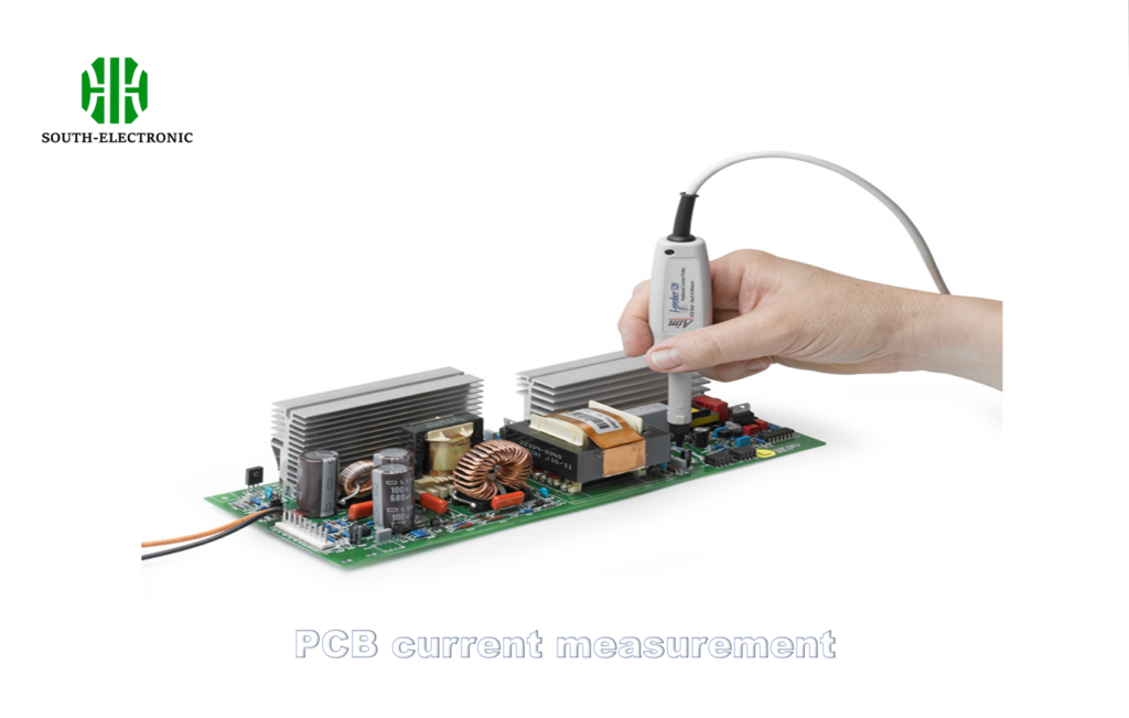
Tired of PCB EMI issues disrupting your electronics? Learn proven ways to fix them.
Ensure PCB design meets EMI standards by grounding, proper power/ground wriring, filtering, reducing loops, avoiding 90° angles, and shielding.
Let me break down each critical step so you can implement these strategies in your next design. I’ve learned these lessons the hard way—now you can skip the mistakes.
How Does Grounding Help Reduce EMI in PCB Design?
A bad ground nearly crashed my first PCB project. Don’t let grounding be your EMI weak spot.
Grounding reduces EMI by creating a low-impedance path. Maximize ground area and use strategic layers for best results.

Why Ground Area Matters
In my first project, I used a tiny ground plane—and the EMI was off the charts. Experts say the larger the ground area, the better it neutralizes emissions. For multi-voltage boards, I now use this approach:
| Ground Strategy | When to Use | Cost Impact | EMI Reduction |
|---|---|---|---|
| Single ground layer | Simple designs | Low | Moderate |
| Segmented ground layers | Multiple voltage domains | Medium | High |
| Full ground plane | High-speed/high-reliability | High | Excellent |
Balancing Cost and Performance
Once, I needed five ground layers but couldn’t afford them. I split the board into three ground zones, each serving two voltage rails. This cut costs by 40% while keeping EMI within specs. Always prioritize high-speed sections when segmenting grounds.
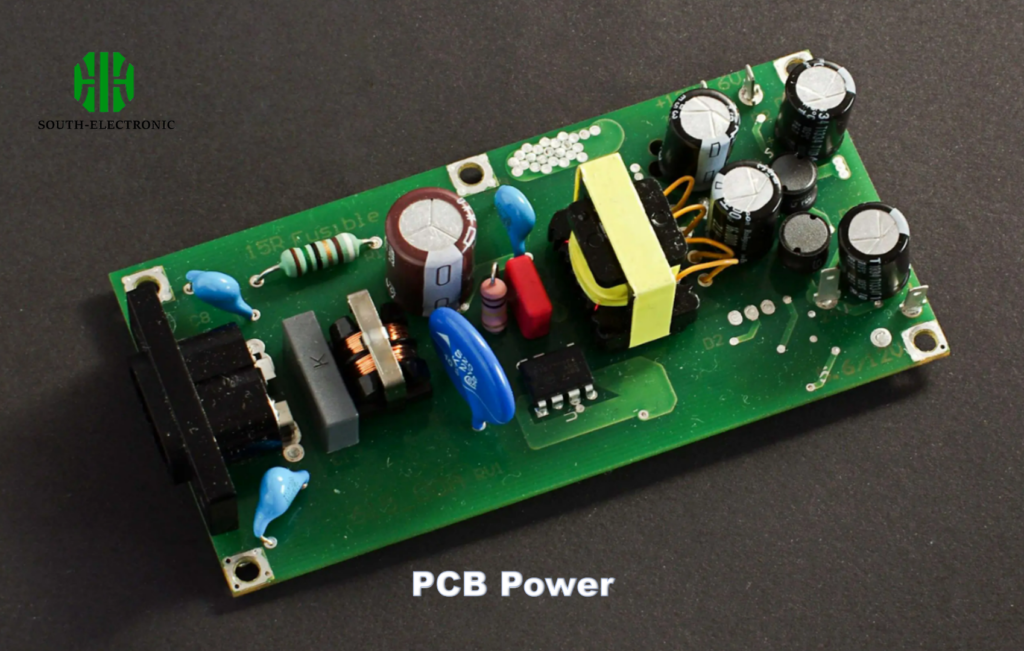
Why Is Power and Ground Wiring Critical for EMI?
I once designed a board with haphazard power routing – it failed EMI testing miserably. Here’s how to route it correctly.
Proper power/ground routing minimizes loops and impedance. Follow width, spacing, and routing rules to reduce EMI.
Key Routing Principles
After that failed project, I swore by these rules:
- Width matters: I make ground traces at least 3mm wide. For a 5A power line, I go to 5mm to reduce resistance.
- Parallel routing: In a recent audio board, parallel power and ground traces cut noise by 60% compared to random routing.
- Closed loops: On a microcontroller board, closing the ground loop shrank voltage differences from 200mV to 30mV.
Multi-Layer Board Tips
In a 4-layer design, I use one layer as a full ground plane. Here’s a table of what works for different board types:
| Board Type | Power/Ground Strategy | EMI Reduction |
|---|---|---|
| 2-layer | Wide parallel traces, ground loops | Moderate |
| 4-layer | Dedicated ground plane, power plane | High |
| 6+ layer | Split power planes over ground planes | Excellent |
How to Use Filtering to Minimize PCB EMI?
Forgot filtering on a WiFi board—signal interference turned it into a brick. Filters are non-negotiable.
Use de-coupling caps, EMI filters, and magnetic components on power/signal lines to block interference.
Filter Types and Placement
- De-coupling caps: On a microprocessor board, placing 0.1μF caps within 5mm of each IC pin cut high-frequency noise by 75%.
- EMI filters: In a USB design, a common-mode choke on the data lines stopped it from interfering with nearby radios.
- Magnetic components: A ferrite bead on a 5V line killed a pesky 200MHz noise spike in my last project.
Filter Selection Table
Use this to pick the right filter:
| Filter Type | Best for | Placement | Cost |
|---|---|---|---|
| Ceramic cap | High-frequency noise | Near IC power pins | Low |
| Electrolytic cap | Low-frequency ripple | Power supply entry | Medium |
| EMI filter module | Broadband noise | Line entry point | High |
| Ferrite bead | Specific frequency spikes | On noisy lines | Low |
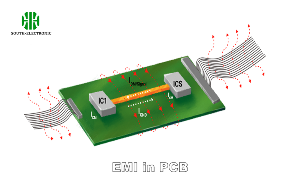
Why Should You Minimize Loop Areas in PCB Design?
A large loop in my first PCB acted like an antenna—radiating enough EMI to fail certification.
Loops act as antennas. Minimize loop count, area, and use single return paths to reduce radiation.
The Loop Antenna Problem
In that failed design, a 10mm x 10mm loop radiated at 868MHz—right into a nearby receiver. Here’s how I fix loops now:
- Single return path: On a sensor board, ensuring each signal had one ground return cut radiation by 80%.
- Power layer use: Using a power plane in a 4-layer board shrank loop areas from 20mm² to 1mm².
- Loop area math: I now calculate loop area with this formula: Area = length x width. Keep it under 1mm² for high-speed signals.
Loop Reduction Techniques
| Technique | How It Works | Impact on EMI | Difficulty |
|---|---|---|---|
| Single return path | Forces one ground route | High | Easy |
| Power/ground planes | Creates low-impedance return | Very high | Medium |
| Differential signaling | Cancels loop radiation | High | Complex |
Why Avoid 90° Angles in PCB Traces?
A PCB with 90° corners failed EMI testing—those angles are radiation hotspots. Here’s why.
90° angles increase capacitance and impedance, causing reflections and EMI. Use 45° angles or arcs instead.
The Science Behind Corner Angles
In a high-speed design, a 90° corner changed the trace impedance from 50Ω to 70Ω—causing 30% signal reflection. Switching to two 45° angles fixed it. Here’s what happens:
- Capacitance increase: 90° corners add extra capacitance, slowing signals.
- Impedance mismatch: This causes signal reflections, which generate EMI.
- Radiation increase: Sharp corners act like small antennas, radiating energy.
Corner Design Options
| Corner Type | Impedance Change | Radiation Level | Ease of Design |
|---|---|---|---|
| 90° angle | High (20-30%) | High | Easy |
| 45° angle | Low (5-10%) | Low | Medium |
| Arc (curved) | Negligible | Very low | Hard |
I now use 45° angles by default. For critical signals (like HDMI), I take the time to route arcs—worth it to pass EMI tests.
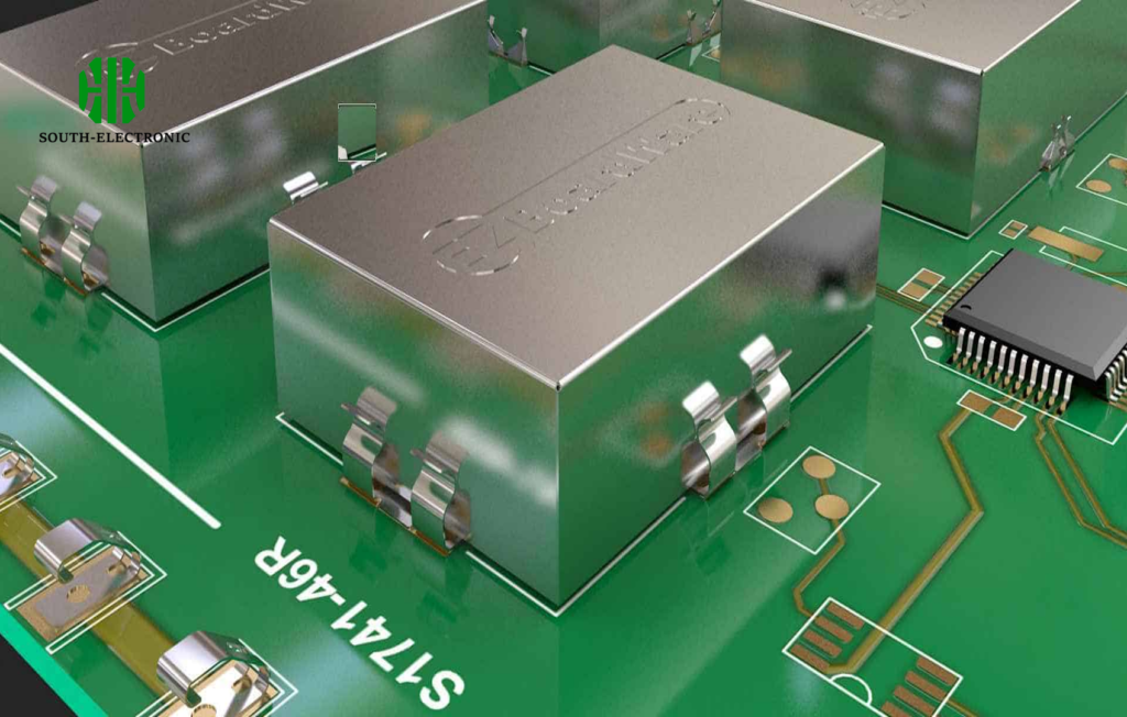
How Do Cables and Shielding Fight PCB EMI?
Unshielded cables turned my robot into a radio jammer. Proper cabling is half the EMI battle.
Use twisted pair or shielded cables, ground shields properly, and add physical shields to contain EMI.
Cable Types and Uses
- Twisted pair: In a data logger, twisted pair cables cut crosstalk by 90% compared to flat cables.
- Shielded cables: A USB 3.0 shielded cable stopped my board from interfering with a Bluetooth module.
- Coaxial cables: For RF signals, nothing beats coax. I learned this after a 2.4GHz antenna failed without it.
Shielding Best Practices
| Shield Type | How to Use | EMI Reduction | Cost |
|---|---|---|---|
| Cable shield | Ground both ends for RF; one end for audio | High | Medium |
| Metal enclosure | Enclose high-EMI sections, ground thoroughly | Excellent | High |
| PCB shield layer | Add a shield layer over sensitive traces | Good | Low |
On a drone project, a metal shield around the flight controller cut EMI enough to keep GPS signals strong—critical for safe flights.
Conclusion
Follow these six steps—grounding, wiring, filtering, loop reduction, corner design, and shielding—to make your PCB EMI-compliant.

