
Ever snapped a PCB mid-project? That cracking sound isn’t just frustration—it’s failed laminate materials screaming. Choosing the wrong base layer destroys circuits before they ever power on. Stop gambling with your board’s foundation. I’ve seen designs implode from this exact oversight.
PCB laminate materials are non-conductive base layers that support circuits and prevent electrical leaks. They’re fiberglass-resin composites pressed together under heat. FR-4 laminate remains popular for its balanced strength and insulation up to 130°C, handling most standard projects reliably.

Laminate choice affects everything – speed, heat resistance, cost. Ignore this and you risk entire batches failing. But knowledge blocks failure. Next, we tackle real-world upgrade decisions preventing millions in losses.
When to upgrade from FR-4 to high-frequency PCB laminates?
Struggling with radio signals dropping? Your FR-4 laminate might suffocate high frequencies. Most designers cling to FR-4 too long, eating signal integrity while cheaper options degrade. I recall reworking a drone controller losing GPS data daily.
Upgrade when signals exceed 500MHz. High-frequency laminates offer stable dielectric properties reducing signal loss 40% over FR-4. They’re essential for 5G networks, aerospace radar, and high-speed servers where heat tolerance exceeds 180°C.
Material Differences That Matter
Three factors force the upgrade: stability, loss rate, and thermal limits.
| Property | FR-4 Laminate | High-Frequency Laminate |
|---|---|---|
| Dielectric Constant | 4.5 (variable) | 3.0-3.5 (stable) |
| Loss Tangent | 0.02 | 0.001-0.004 |
| Max Temp | 130°C | 180°C+ |
| Cost Increase | – | 2-4x |
Signal drift occurs with FR-4’s inconsistent dielectric constant (Dk), causing timing errors in GHz transmissions. The high loss tangent (Df) bleeds energy as heat, weakening transmissions. For satellite comms or millimeter-wave applications, FR-4’s thermal ceiling risks delamination during reflow soldering. Polyimide or PTFE laminates maintain stable Dk/Df even at extreme heat, preserving signal accuracy where FR-4 crumbles. However, costs surge 300%, so weigh budgets against circuit lifespan.
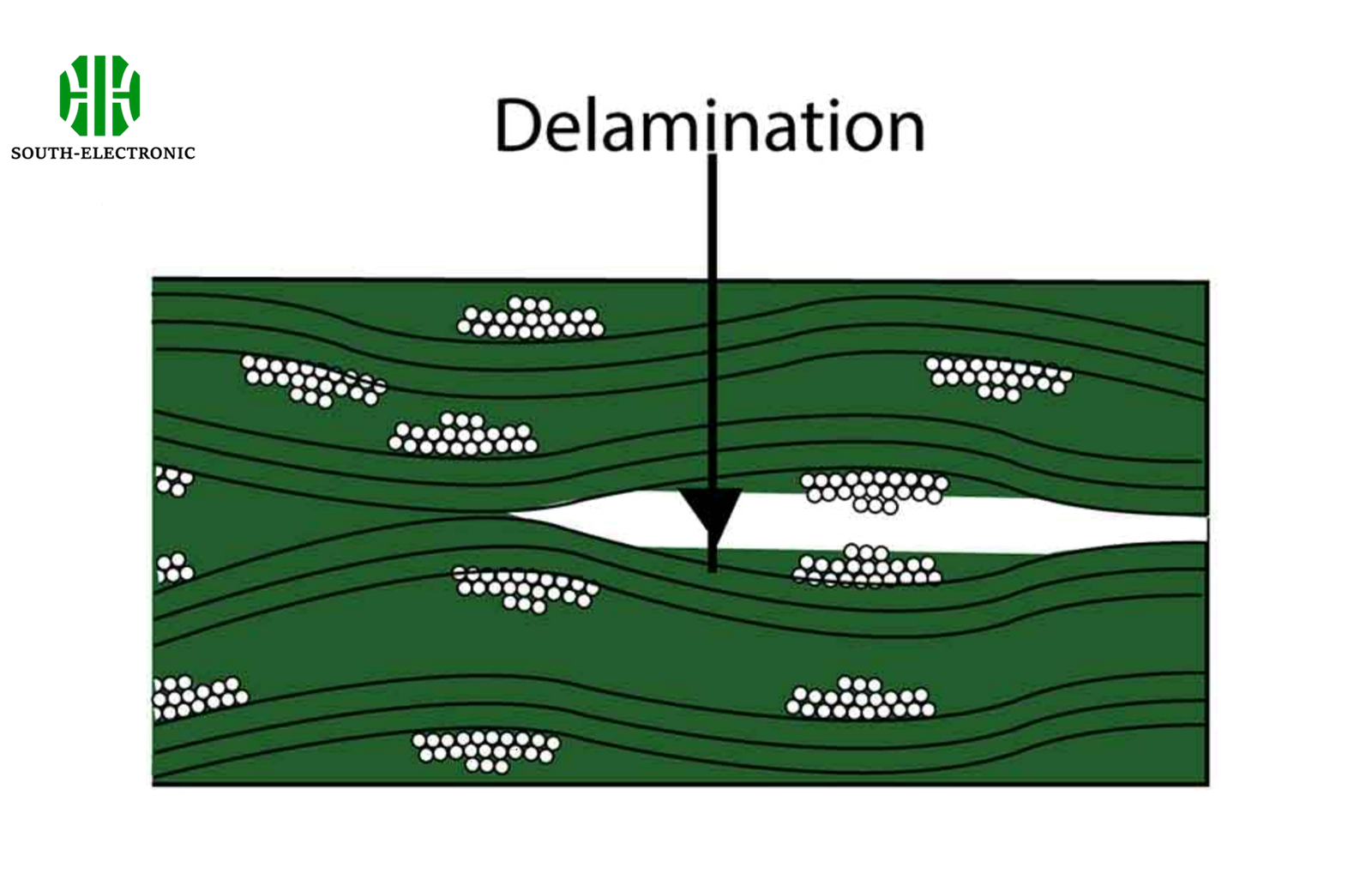
How does the PCB lamination process prevent delamination and CAF failure?
Found white cracks between copper layers? That’s delamination inviting catastrophes like CAF (conductive anode filament) growth. Moisture creeps into gaps, forming metal dendrites which bridge circuits. Entire server farms failed due to skipped lamination steps.
Lamination fuses layers under heat/pressure, eliminating air pockets where moisture forms. Using low-CTE materials and precise resin flows blocks gaps, preventing CAF growth paths and structural weakness.
Three Failure Prevention Strategies
The battle hinges on pressure control, chemistry, and moisture barriers.
| Step | Common Error | Optimization |
|---|---|---|
| Material Prep | Skipping pre-dry | Bake 2hrs @110°C |
| Resin Flow Control | Uneven pressure | Multi-zone press control |
| Cooling Rate | Rapid temperature drop | Gradual 5°C/min descent |
Delamination starts when trapped air expands during soldering. Forced heating cycles (like reworking boards) compounds this. By vacuum-sealing layers while injecting calibrated resin, bubbles evacuate. Low thermal-expansion materials (like ceramic-filled FR-4) flex less under thermal stress, eliminating crack nucleation points. CAF prevention requires resin to seal glass fibers tightly – any gap allows copper ions to migrate in humid conditions. Using brominated flame retardants instead of chlorinated improves moisture resistance while ionic purity tests on pre-pregs kill conductive pathways before assembly begins.
What are the 6 critical factors for choosing PCB laminate thickness?
Ever plugged a RAM stick into a flexed motherboard? Improper thickness warps entire batches. Manufacturers often fixate on cost per square inch, overlooking stack-up impacts. I once scrapped 500 boards due to 0.1mm thickness mismatch on impedance traces.
Choose thickness based on layer count, copper weight, impedance targets, component types, fabrication constraints, and flex requirements. Thinner laminates suit complex 8+ layer boards, while thicker ones handle high-current traces.

Engineering Tradeoffs Explained
Your layer stack determines everything – from signal loss to assembly yield.
| Factor | Thin Laminate (1.5mm) | |
|---|---|---|
| Layer Capacity | 8-20 layers | 2-4 layers |
| Impedance Control | ±5% tolerance | ±10% tolerance |
| Heat Dissipation | Limited airflow | Excellent thermal mass |
| Vibration Resistance | Low (flex) | High (rigid) |
Impedance demands precision – a 100Ω trace requires exact dielectric spacing. Thin laminates achieve ±5% tolerance crucial for USB/PCIe interfaces. However, high-power designs (motor controllers, PSUs) need thick cores to support heavy copper (≥2oz/ft²) without delaminating during solder reflow. Flex boards force thickness compromises – mobile devices use 0.2mm to bend, while industrial controllers tolerate 2mm. Consult fabricators first: standard thicknesses (1.0mm, 1.6mm) cost 30% less due to optimized tooling, whereas custom specs increase delays.
Conclusion
Your PCB laminate material choice decides reliability. Upgrade when signal speeds exceed FR-4 limits. Master lamination processes to dodge delamination. Balance six thickness factors for stable performance.

