
Tired of cracked edges and material limitations in your PCB production? Traditional cutting methods struggle with delicate materials and intricate designs. PCB laser cutting solves this with contactless precision, enabling cleaner cuts and complex shapes without mechanical stress.
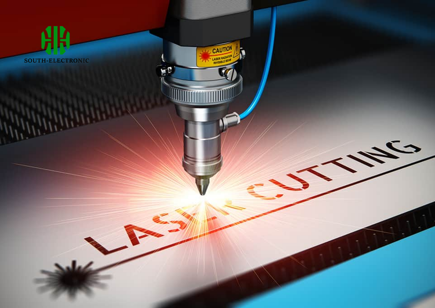
PCB laser cutting[^1] uses focused light beams to vaporize copper and substrate materials, creating precise circuit board patterns. This non-contact method[^2] achieves ±25μm accuracy, eliminates tool wear, and handles flexible PCBs better than mechanical methods.
Let’s examine how this technology transforms board fabrication through three key aspects:
How Does PCB Laser Cutting Work?
Wondering how light becomes a cutting tool? Lasers overcome material limitations better than blades. The process combines science and engineering for board shaping.
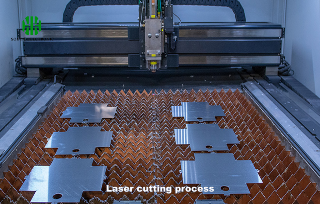
PCB lasers use amplified light beams focused through lenses to ablate material layer by layer. CO2 lasers cut organic substrates, while fiber lasers[^3] handle metals. Computer-controlled mirrors guide the beam across predefined paths.
)
The Precision Dance: From Design to Cut
Laser systems require three coordinated components:
-
Beam Generation
CO2 (10.6μm wavelength) for FR-4
Fiber (1.06μm) for thin copper layers -
Motion Control
Galvanometer mirrors steer beams at 5m/s speeds
XY platforms position boards -
Material Interaction
Instant vaporization at 100-300W power
Burnt edges cleaned with gas assist
| Parameter | CO2 Laser | Fiber Laser |
|---|---|---|
| Wavelength | 10.6 μm | 1.06 μm |
| Best For | Organic boards | Metal-heavy PCBs |
| Cutting Speed | 2-3 m/min | 8-10 m/min |
| Edge Finish | Slight Charring | Cleaner edges |
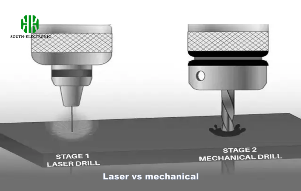
Why Use Lasers Instead of V-Scoring or Punching?
Mechanical methods fail complex designs. Chips crack. Tools wear out. Lasers avoid these limitations through non-contact processing.
Lasers outperform v-scoring/punching in fine-pitch applications. They eliminate mechanical stress, handle 0.2mm micro-vias, and enable 45° internal cuts for flexible circuits. No blade replacement reduces downtime.
)
The Tradeoff Matrix
Compare methods across four critical factors:
| Criteria | V-Scoring | Punching | Laser Cutting |
|---|---|---|---|
| Minimum Cut Width | 500μm | 800μm | 25μm |
| Material Loss | 200-300μm kerf | 500μm+ burrs | 20μm heat zone |
| Setup Time | 15-30 mins | 2-4 hours | 5-10 mins |
| Recurring Cost | Blade changes | Die maintenance | Electricity |
Laser’s initial $80k-$250k investment pays off when cutting >5,000 boards/month. Prototyping shops save 40% time vs mechanical methods.
What Materials Can Be Cut with PCB Lasers?
Not all boards survive the laser. Material composition determines cutting quality and speed. Some require special settings.
Lasers effectively cut FR-4[^4], polyimide, ceramic, and PTFE substrates. Avoid halogen-rich materials – chlorine/bromine release toxic fumes. Copper thickness below 2oz works best.
)
Material Guide for Engineers
| Material | Laser Type | Max Thickness | Notes |
|---|---|---|---|
| FR-4 (Standard) | CO2 | 1.6mm | Reduce power for thin layers |
| Flexible PI | Fiber | 0.2mm | Avoid stretching during cut |
| Aluminum-Clad | Fiber | 3.0mm | Reflectivity issues below 30W |
| Ceramic (AlN) | CO2/Fiber Mix | 0.8mm | Requires oxygen assist gas |
For Rogers 4350B high-frequency boards, use 20% reduced power to prevent delamination. Always test settings on scrap material first.
Conclusion
PCB laser cutting delivers unmatched precision for complex designs and soft substrates, though costs may limit low-volume use. As electronics miniaturize, mastering this technology becomes crucial for advanced PCB manufacturing.
[^1]: Explore the advantages of PCB laser cutting, including precision and material versatility, to enhance your PCB production process.
[^2]: Learn how non-contact methods like laser cutting can revolutionize PCB manufacturing by reducing stress on materials and improving accuracy.
[^3]: Discover the role of fiber lasers in PCB cutting, especially for metal-heavy designs, and how they enhance production efficiency.
[^4]: Discover the significance of FR-4 in PCB manufacturing and its properties that make it a popular choice among engineers.

