

Ever struggled with drilling microscopic holes in modern electronics? Circuit boards keep shrinking while performance demands soar. Laser drilling solves this precision paradox for next-gen devices.
Laser drilling[^1] uses focused light beams to vaporize PCB material, creating holes as small as 10µm. This non-contact method eliminates tool wear, enables complex via shapes, and handles delicate materials mechanical drills can’t process.
While lasers sound futuristic, their real-world implementation involves specific technical decisions. Let’s dissect four critical aspects that determine laser drilling’s effectiveness across different applications.
What Makes Laser Drilling Superior to Mechanical Drilling for High-Density PCBs?
Mechanical drills distort materials when creating 200µm holes. Modern high-density interconnects[^2] require holes five times smaller – precisely where lasers excel.
Laser drilling outperforms mechanical methods for holes below 150µm, achieving ±5µm positional accuracy without physical tool contact. It prevents material delamination in thin substrates and enables staggered microvias for 3D packaging.
)
Key Technical Differentiators
| Parameter | Laser Drilling | Mechanical Drilling |
|---|---|---|
| Minimum Hole Size | 10µm | 100µm |
| Aspect Ratio | 1:1 | 8:1 |
| Material Flexibility | FR4 to Polyimide | Limited to rigid substrates |
| Tool Wear | None | Frequent bit replacement |
| Hole Geometry | Tapered/Shaped Vias | Cylindrical Only |
HDI designs demand 20-50µm dielectric layers between copper planes. Mechanical drilling creates stress fractures in these thin prepreg layers – I’ve seen 30% rejection rates on 6-layer smartphone boards. CO2 lasers pulse at 9.4µm wavelength, selectively ablating glass fibers while preserving surrounding resin.
UV lasers[^3] (355nm) handle different challenges. Their shorter wavelength targets organic materials cleanly. A recent IoT module project required 80µm holes through 12µm copper + 50µm FR4. UV lasers achieved 85% first-pass yield versus 55% with mechanical alternatives.
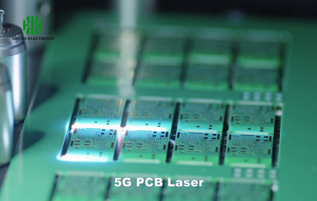
What Precision Parameters Define Successful Laser Drilling in 5G Applications?
Miss by 5µm in 5G antenna arrays[^4]? You’ve just halved signal integrity. Millimeter-wave PCBs demand unprecedented drilling accuracy.
Critical parameters are spot size (≤25µm), pulse overlap (85-92%), and positional accuracy (±3µm). Frequency-doubled Nd:YAG lasers maintain 1-5µm repeatability across 600mm panels, essential for 28GHz phased arrays.
)
5G-Specific Process Control
| Parameter | Target Range | Measurement Method |
|---|---|---|
| Beam Diameter | 20±2µm | CCD Camera Analysis |
| Pulse Energy | 0.8-1.2mJ | Pyroelectric Sensor |
| Hole Taper | <5° | Cross-Section SEM |
| Copper Residue | 120kHz | |
| Backside CCD | Exit Hole Diameter | 105-115% Entry Diameter |
| Gas Chromatography | Ablation Byproducts | CO2 Levels <200ppm |
| X-Ray Inspection | Plating Uniformity | Copper Thickness ≥18µm |
| Thermal Shock Testing | Via Reliability | 500 Cycles (-40°C/+125°C) |
In 5G power amplifiers, thermal management vias[^5] must align precisely with GaN dies. I worked on a base station board requiring 2000+ 35µm holes per square inch. Implementing real-time Z-axis compensation reduced depth variation from ±8µm to ±3µm across warped substrates.
Material selection matters too. Rogers 4350B’s ceramic-filled hydrocarbon requires different pulse settings than standard FR4. Through testing, we found 15% lower pulse energy prevents microcracks in high-frequency laminates.
Can Laser Drilling Economics Compete with Traditional Methods Beyond Miniaturization?
Upfront laser costs deter many manufacturers. But hidden savings emerge in high-volume production of complex designs.
Laser drilling becomes cost-effective at 5,000+ holes/panel due to zero tooling costs. For 18-layer server boards with 20,000 vias, laser processing reduces total cost by 40% versus mechanical plus plasma desmear.
)
Total Cost Breakdown (100 Panel Batch)
| Cost Factor | Laser Drilling | Mechanical Drilling |
|---|---|---|
| Equipment Depreciation | $12/panel | $8/panel |
| Consumables | $1.50/panel | $4.20/panel |
| Rework | 2% panels | 8% panels |
| Cycle Time | 45min/panel | 68min/panel |
| Energy Cost | $3.10/panel | $2.80/panel |
A recent automotive radar project showed lasers’ hidden value. Mechanical drilling required separate drilling/desmear steps with 12-hour turnaround. Laser ablation created clean, smear-free holes in single pass, cutting total processing time by 35%. For JIT manufacturing, this workflow advantage outweighed higher hourly rates.
What In-Process Monitoring Ensures Laser-Drilled Via Reliability in Automotive Electronics?
A single flawed via can disable an entire ADAS module. Real-time monitoring bridges the gap between laboratory precision and mass production.
Three-layer monitoring combines: 1) Plasma emission spectroscopy for material breakthrough detection 2) IR thermography for heat-affected zone control 3) Confocal height mapping for depth uniformity±2µm.
)
Automotive-Grade QC Measures
| Monitoring Method | Parameter Measured | Acceptance Criteria |
|---|---|---|
| Laser-Induced Acoustic | Hole Completion | Frequency Shift >120kHz |
| Backside CCD | Exit Hole Diameter | 105-115% Entry Diameter |
| Gas Chromatography | Ablation Byproducts | CO2 Levels <200ppm |
| X-Ray Inspection | Plating Uniformity | Copper Thickness ≥18µm |
| Thermal Shock Testing | Via Reliability | 500 Cycles (-40°C/+125°C) |
For electric vehicle battery modules, we implemented edge AI analyzing plasma spectra in real-time. The system automatically adjusted pulse frequency when detecting varying copper thickness – reducing voids from 7% to 0.8% across temperature-sensitive Nickel substrates.
Conclusion
Laser drilling enables PCB innovations through unmatched precision and flexibility. As 5G/EV demands grow, combining optimized parameters, economic analysis, and smart monitoring ensures reliable, cost-effective microvia production at scale.
[^1]: Explore the benefits of laser drilling in electronics to understand its impact on precision and efficiency in modern manufacturing.
[^2]: Learn about high-density interconnects to grasp their role in advancing PCB technology and performance.
[^3]: Explore how UV lasers enhance precision drilling, especially in applications like 5G, ensuring high yield and accuracy.
[^4]: Learn about the critical impact of drilling accuracy on 5G antenna arrays and overall signal integrity.
[^5]: Discover the role of thermal management vias in optimizing performance and reliability in power amplifiers.

