
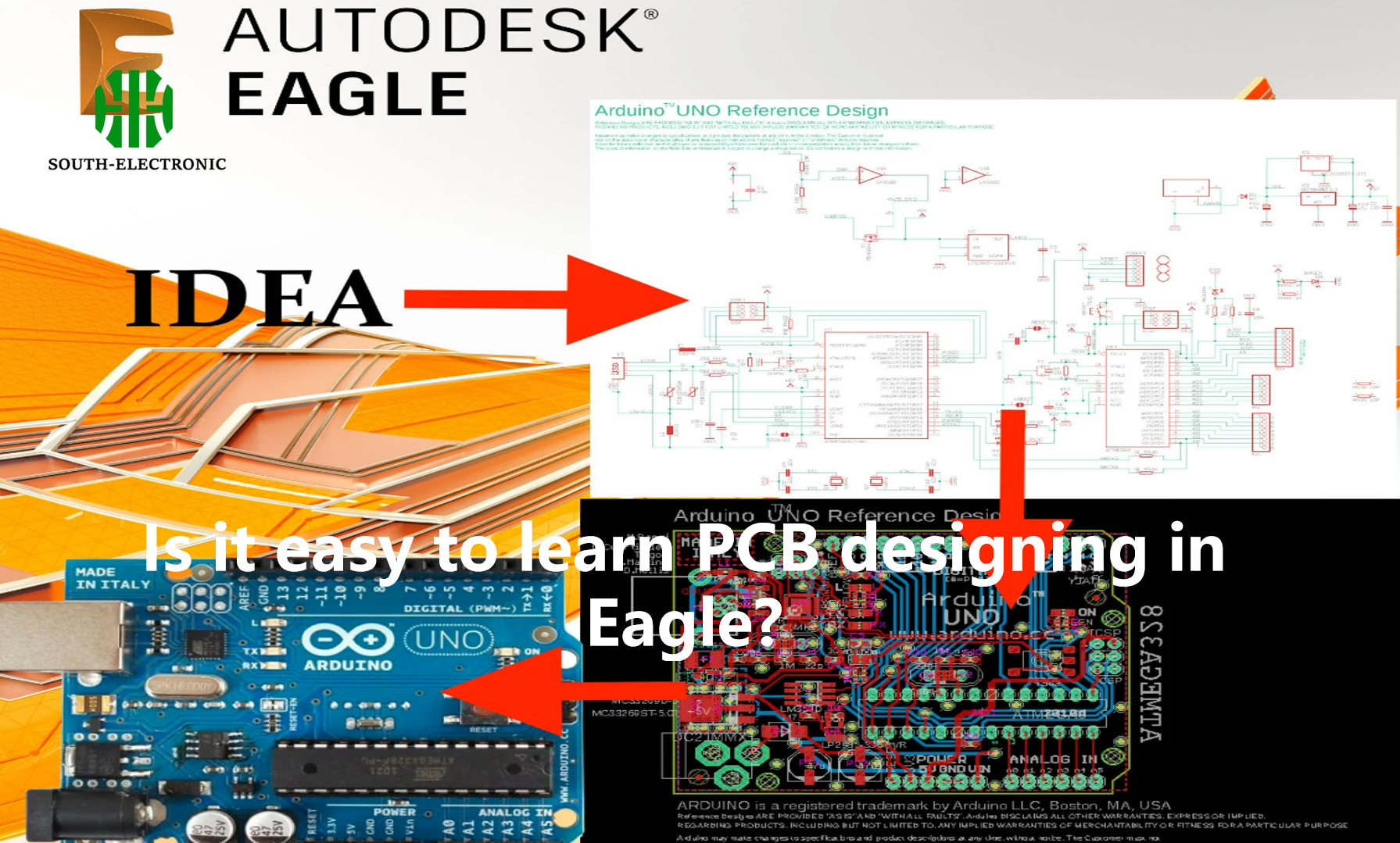
Is it easy to learn PCB designing in Eagle?
A lot of people ask me if they can learn to design PCBs using Autodesk Eagle. They look at all the features and get overwhelmed. They think it’s going to be really hard to learn. But I’m here to tell you that it’s not that hard. With a little bit of guidance and some practice, you can learn to design PCBs in Eagle. It’s not that bad. It’s actually kind of fun.
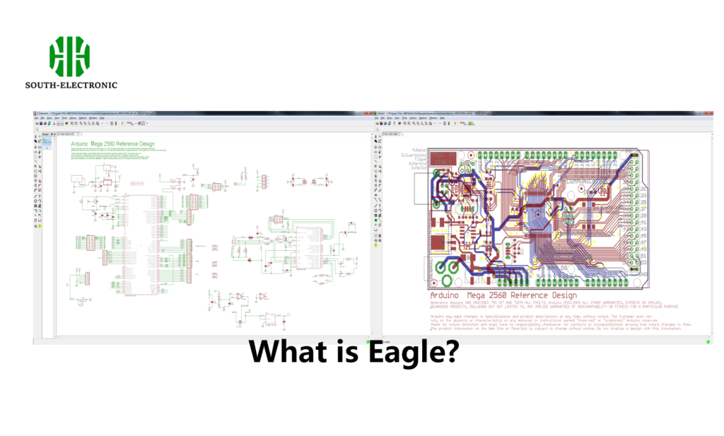
What is Eagle?
Eagle, which stands for “Easily Applicable Graphical Layout Editor,” is a powerful software used for designing printed circuit boards (PCBs). With Eagle, you can create schematics, design PCB layouts, and generate manufacturing files. It’s a popular choice among hobbyists, students, and professionals because it’s easy to use, has a large library of parts, and is more affordable than other PCB design tools.
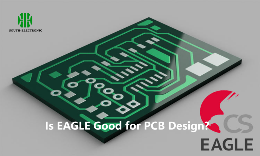
Is EAGLE Good for PCB Design?
Yes, Eagle is an excellent tool for PCB design. It’s widely used in the industry and offers a seamless connection between schematic diagrams, component placement, and PCB routing. The software is versatile and capable of handling simple to complex PCB designs. Moreover, Eagle’s vast component library and community support make it easier for users to find the necessary components for their projects.
Advantages of Using Eagle for PCB Design:
User-Friendly Interface:
- Eagle’s interface is intuitive, making it easier for beginners to start designing PCBs without a steep learning curve.
Extensive Library Support:
- Eagle provides access to a vast library of components, reducing the time spent on custom part creation.
Cross-Platform Compatibility:
- Eagle is available on Windows, macOS, and Linux, allowing users to work on their preferred operating systems.
Active Community and Resources:
- The active online community provides tutorials, forums, and guides that are immensely helpful for both beginners and advanced users.
Is PCB Design Hard to Learn?
Learning PCB design can be tough, especially if you’re new to electronics. But Eagle makes it easy with its user-friendly tools and extensive support resources. It might take you 6-8 months to get good at PCB design, but mastering it might require a deeper understanding of electronics and circuit design.
Challenges in Learning PCB Design:
- Understanding Circuit Design:A solid understanding of circuit design is crucial for effective PCB design. Beginners may need to invest time in learning basic electronics principles.
- Component Placement and Routing:Correctly placing components and routing connections is essential for a functional PCB. Eagle’s design rules help users avoid common mistakes during this process.
- Design for Manufacturability (DFM):Ensuring that the PCB design can be manufactured efficiently and cost-effectively is another challenge. Eagle offers tools that help in DFM analysis.
Comparison of Learning Curves for Popular PCB Design Software
| Software | Learning Curve | User Interface | Community Support | Cost |
|---|---|---|---|---|
| Eagle | Moderate | Intuitive | Active | Affordable |
| Altium Designer | Steep | Professional | Extensive | Expensive |
| KiCad | Moderate | User-friendly | Active | Free |
| EasyEDA | Easy | Simple | Moderate | Free/Paid |

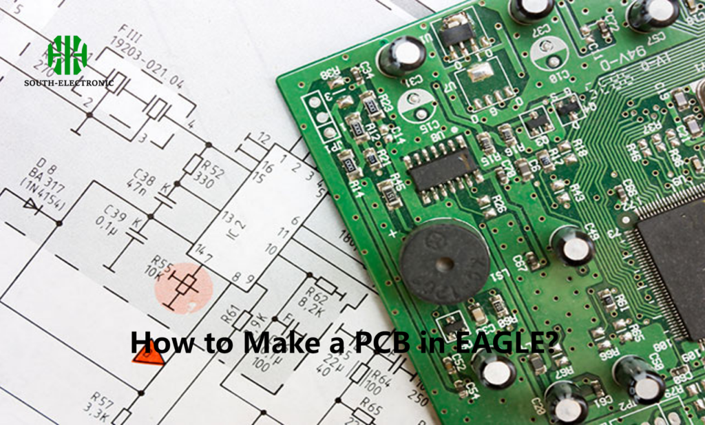
How to Make a PCB in EAGLE?
Creating a PCB in Eagle involves several steps, from schematic design to generating the final Gerber files for manufacturing. Here’s a brief overview of the process:
Step-by-Step Guide to PCB Design in Eagle:
- Download and Install Eagle:Start by downloading and installing Eagle from Autodesk’s website.
- Create a New Project:Open Eagle and create a new project. This will house your schematic and board layout.
- Design the Schematic:Use Eagle’s schematic editor to design the circuit. Add components from the library, connect them using wires, and assign footprints for the PCB.
- Switch to Board Layout:Once the schematic is complete, switch to the board layout view. Arrange the components on the PCB, ensuring optimal placement for routing.
- Route the PCB:Use Eagle’s autorouter or manually route the connections between components. Pay attention to design rules and signal integrity.
- Generate Gerber Files:After routing is complete, generate the Gerber files. These files are used by manufacturers to fabricate the PCB.
- Review and Validate:Before sending the files for manufacturing, review the design using Eagle’s DRC (Design Rule Check) and ERC (Electrical Rule Check) tools.
Tips for Beginners
If you’re new to PCB design, here are some tips to help you get started with Eagle:
- Start with Tutorials: Begin with beginner-friendly tutorials that walk you through the basics of schematic design and PCB layout.
- Use Design Rule Checks (DRC): Always run DRC to catch potential design issues before manufacturing.
- Practice Regularly: The more you practice, the more comfortable you will become with the software. Try designing different types of circuits to broaden your skills.
- Leverage Community Resources: Don’t hesitate to ask questions in forums or seek help from the online community. It’s a valuable resource for troubleshooting and learning.
Resources for Learning Eagle:
To further enhance your learning experience, here are some recommended resources:
- SparkFun Tutorials:A series of tutorials covering everything from basic to advanced PCB design in Eagle.
- Autodesk Eagle Forum:An active community where you can ask questions and get help from experienced users.
- YouTube Channels:Channels like “Jeremy Blum” and “GreatScott!” offer step-by-step video tutorials on using Eagle for PCB design.
- Books:“Make Your Own PCBs with EAGLE: From Schematic Designs to Finished Boards” by Simon Monk is a great resource for learning Eagle.
Learning PCB design in Eagle is not only feasible but also relatively straightforward with the right approach. The software’s user-friendly interface, extensive resources, and active community support make it an excellent choice for beginners and seasoned designers alike. By following the steps and utilizing the resources mentioned in this article, you can confidently start your journey in PCB design using Eagle.

