
High-quality PCBs combine precision processes (photolithography, lamination, plating) with stringent testing. While traditional etching suits simple prototypes, industrial methods enable multi-layer boards, fine pitches (<4 mil), and reliability. Critical factors: material selection, automated inspection, and eco-friendly waste management. Modern designs demand advanced techniques for miniaturization, signal integrity, and thermal performance.
Traditional Etching Method (Simplified Student Prototyping)
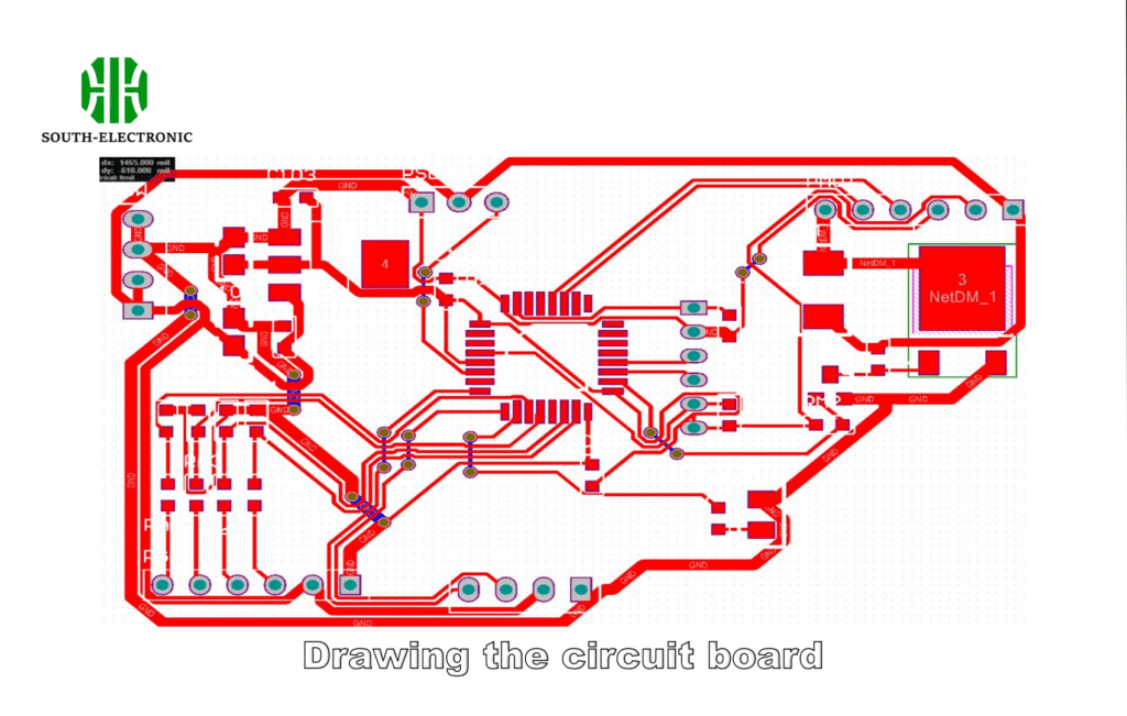
- Design: Use tools like Altium Designer (AD) to create the PCB layout.
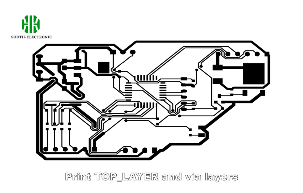
- Printing: Print the TOP_LAYER and via layers onto heat-transfer paper using a laser printer.
- Transfer: Attach the printed design to a copper-clad board using a heat press (20 seconds).
![]()
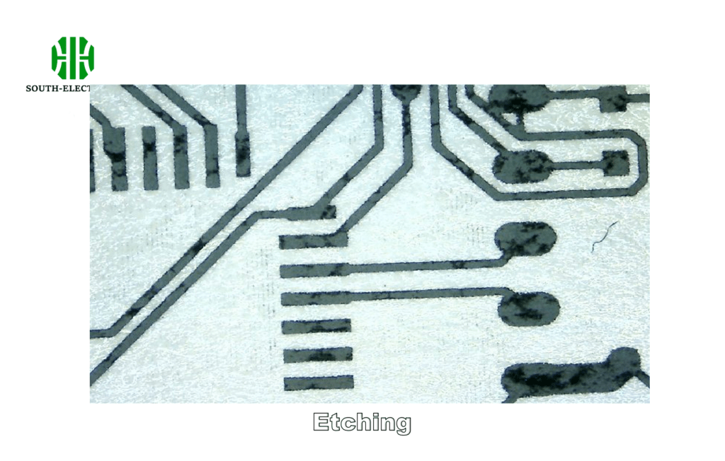
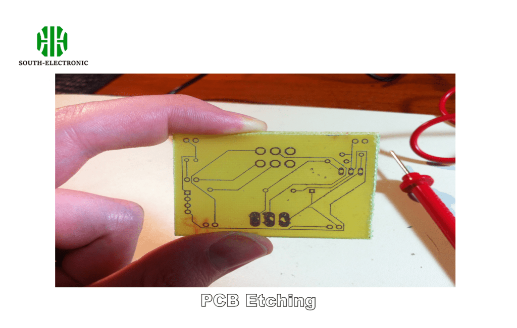
- Etching: Immerse the board in a HCl-H₂O₂ solution in a shaking tank (15 seconds) to remove excess copper. Caution: Corrosive!
-
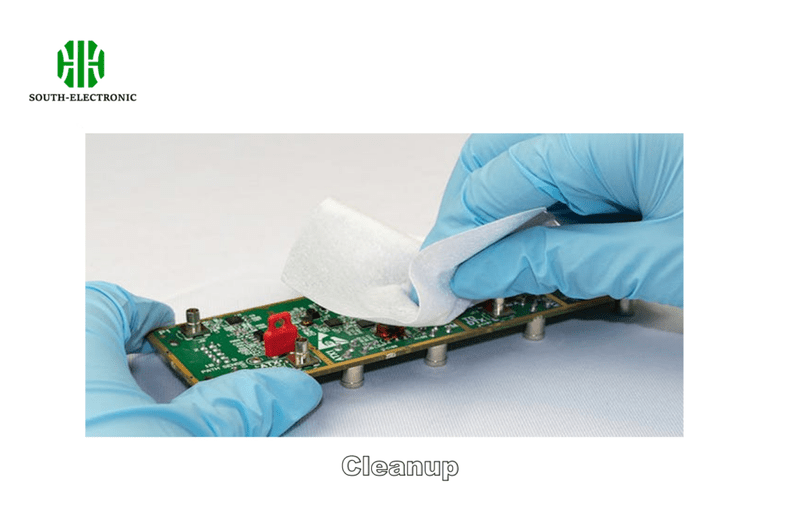
Cleanup: Remove ink with acetone or a steel brush; drill holes as needed.
-
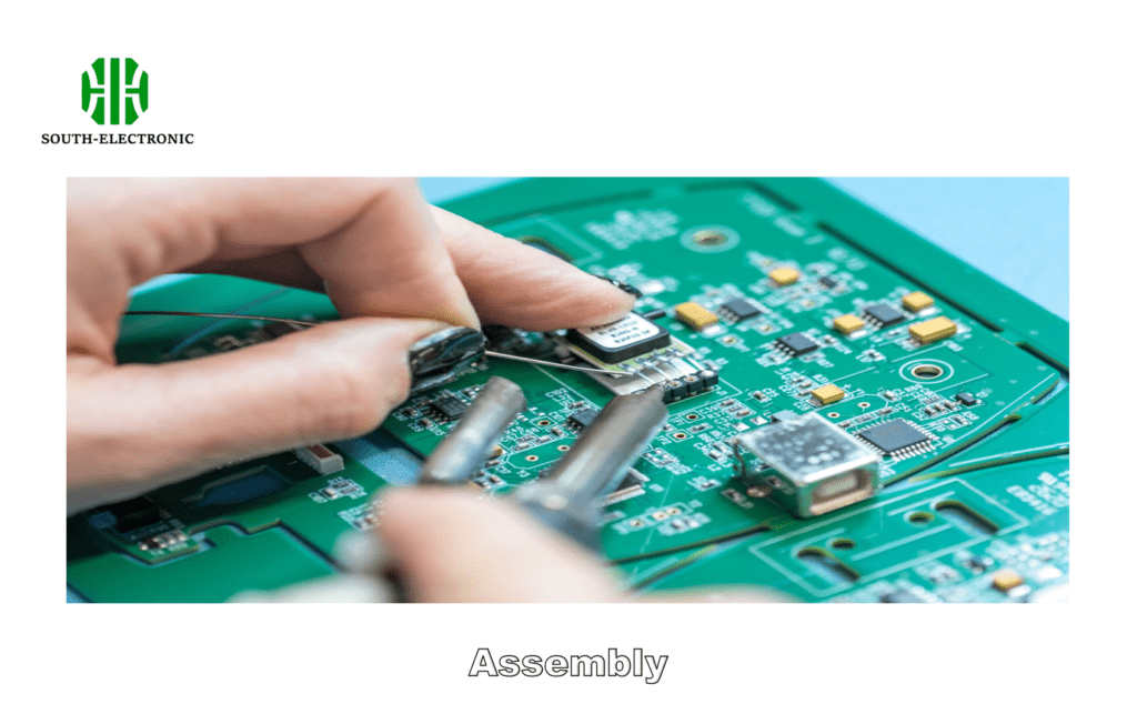
Assembly: Apply flux, pre-tin traces, solder components, clean with solvent, and test.
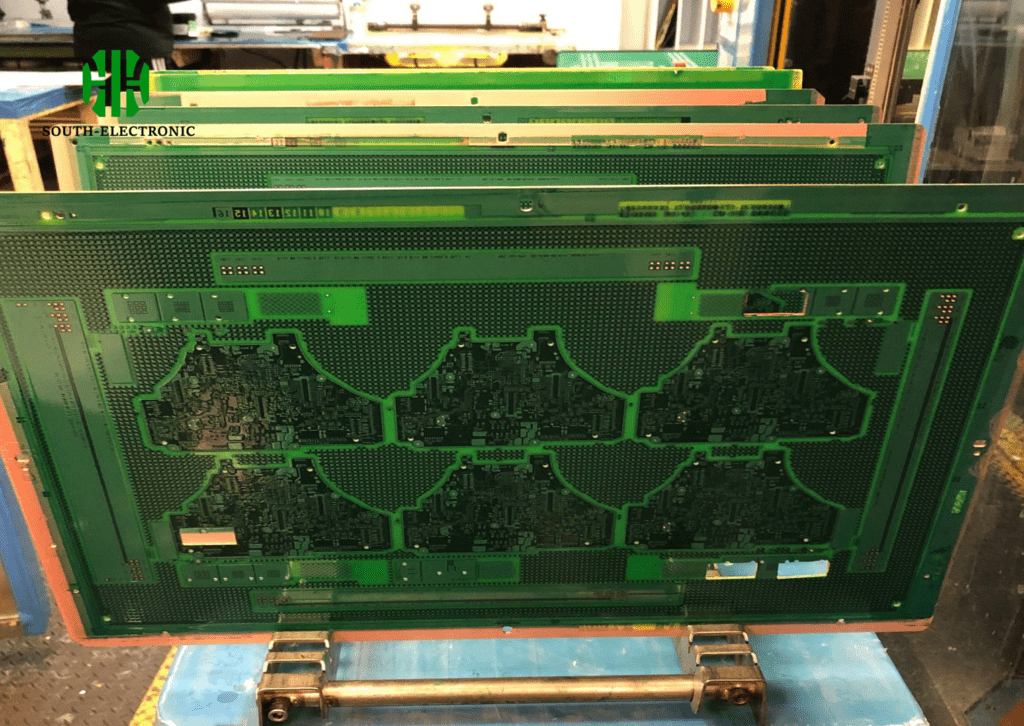
Industrial High-Quality PCB Manufacturing Process
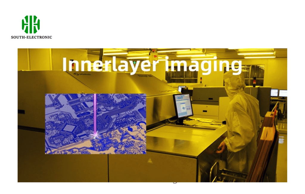
- Inner Layer Imaging: Coat copper laminate with photoresist, expose to UV light through film, develop to reveal circuitry.
- Etching: Remove unwanted copper chemically, strip resist, inspect for defects.
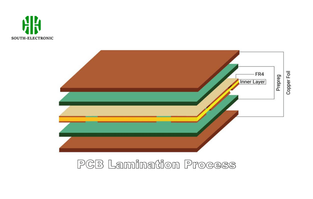
- Lamination: Stack layers with prepreg, apply heat/pressure to bond.
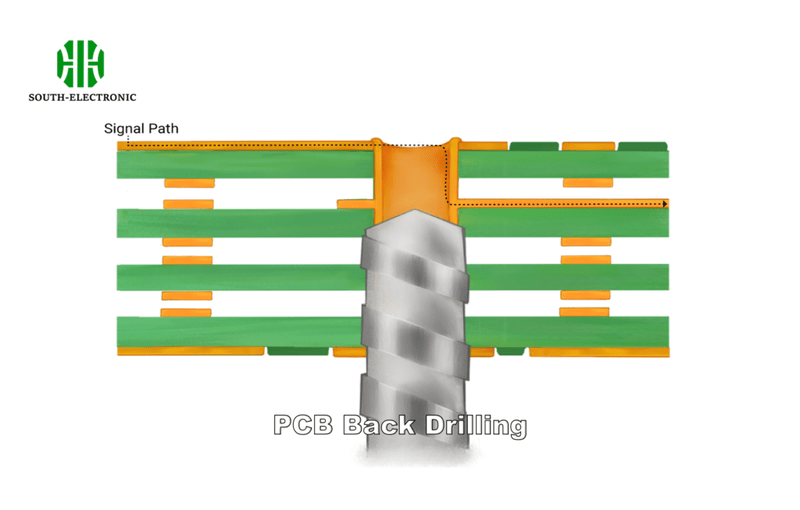
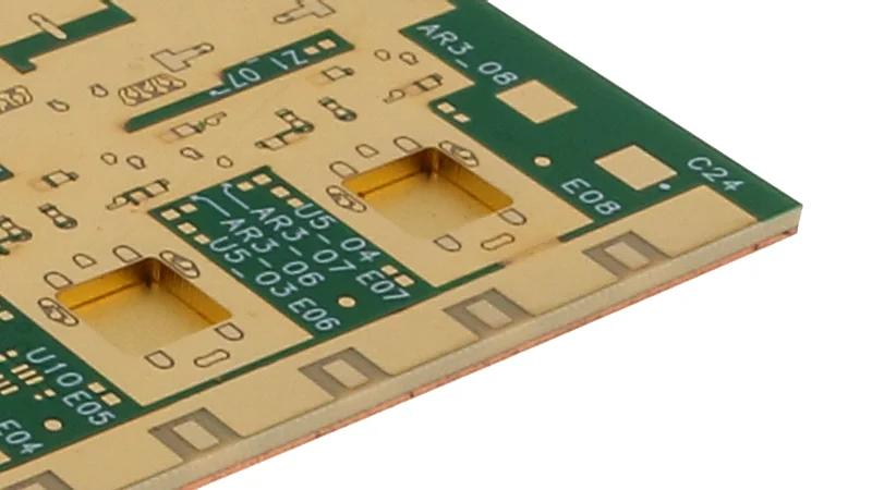
- Drilling: Precision CNC drills micro-vias and through-holes.
- Plating: Electroless/electrolytic copper deposition for conduction.
-
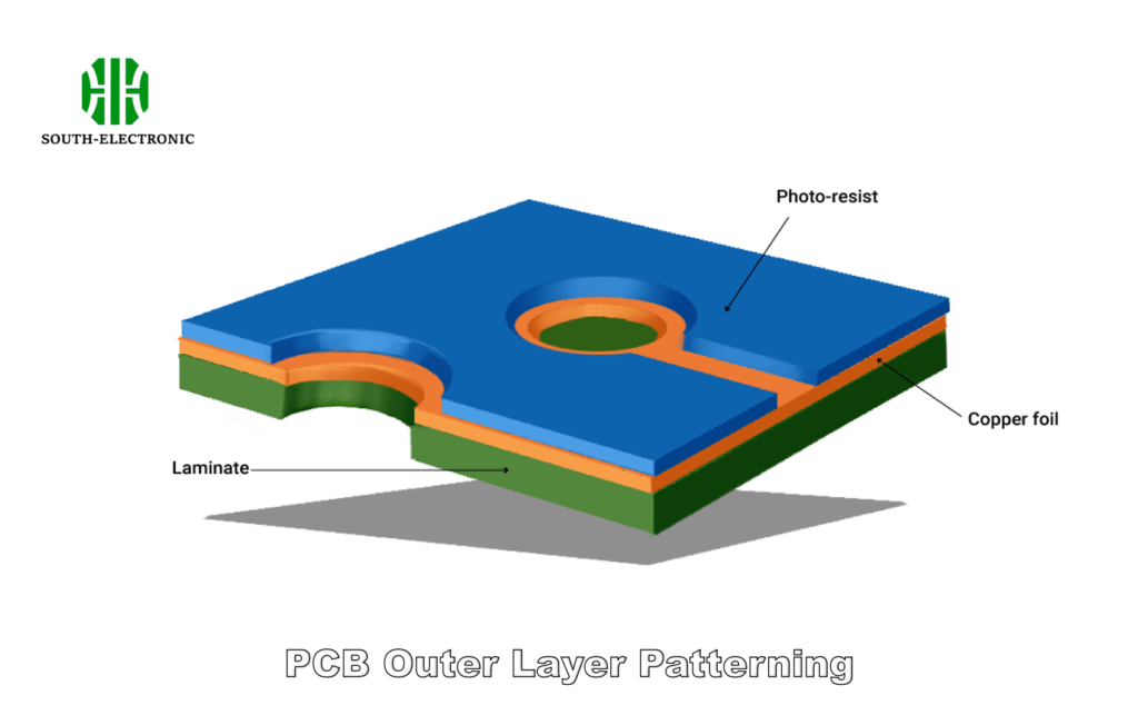
Outer Layer Patterning: Apply dry film, expose/develop, plate tin, etch excess.
-
Solder Mask & Silkscreen: UV-cured epoxy coating, component labels.
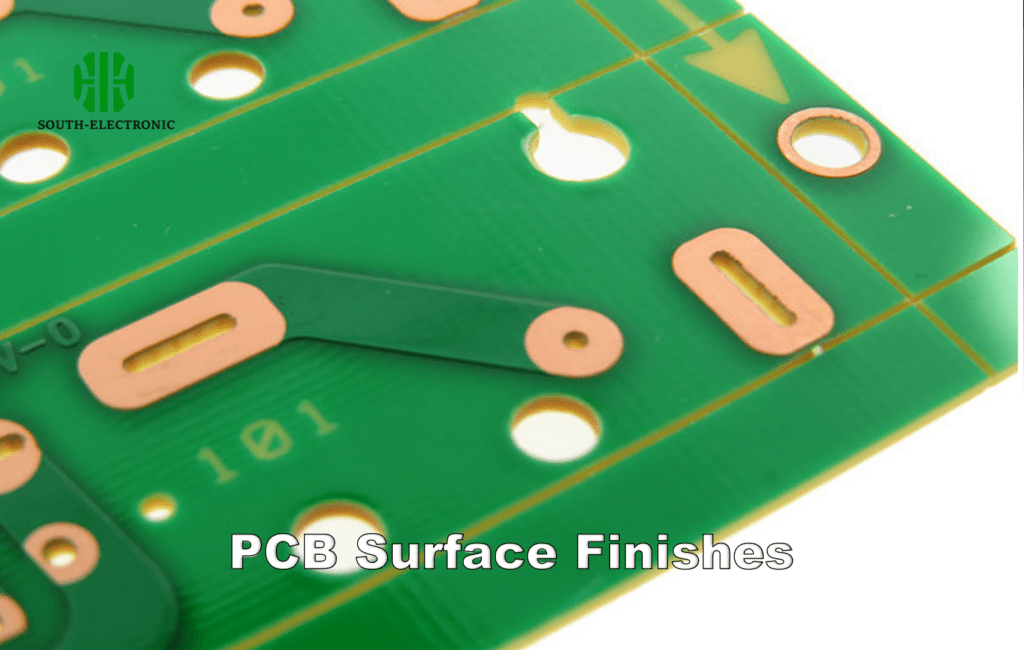
- Surface Finish: ENIG, HASL, or OSP for oxidation resistance.
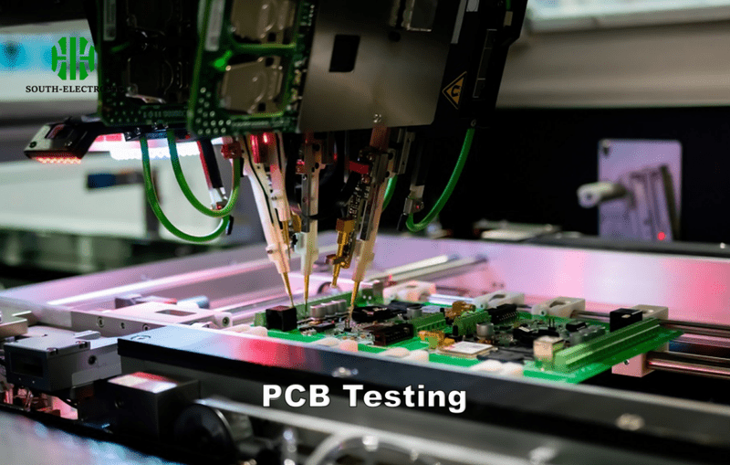
- Testing: Electrical validation (flying probe, AOI).
Modern PCB manufacturing transitions from traditional etching to precision processes, balancing miniaturization, signal integrity, and thermal efficiency to meet rising demands for compact, reliable electronics across cutting-edge applications.


