To minimize reflections during high-speed signal transmission, impedance matching must be maintained at the signal source, receiver, and transmission line. The specific impedance of a single-ended signal line depends on its width and position relative to the reference plane. The width and spacing between differential pairs meeting specific impedance requirements depend on the selected PCB stackup structure.
Since the minimum width and spacing depend on the PCB type and cost requirements, the selected PCB stackup structure must meet all impedance requirements on the board, including inner and outer layers, single-ended and differential lines, and so on.
Layer Definition Design Principles
-
Layers adjacent to the main chip should be ground planes, providing a reference plane for device-side routing.
-
All signal layers should be adjacent to the ground plane whenever possible.
-
Avoid direct proximity between two signal layers.
-
The main power supply should be adjacent to its corresponding layer whenever possible.
-
In principle, a symmetrical design should be adopted. Symmetry includes: dielectric layer thickness and type, copper foil thickness, and pattern distribution type (large copper foil layer, circuit layer).
PCB Layer Definition Recommendations
When setting up specific PCB layers, it’s important to flexibly apply the above principles and determine the layer layout based on actual needs. Avoid rigid imitation. The following are common layer layout recommendations for reference. When setting up layers, if there are adjacent routing layers, reduce crosstalk by increasing the spacing between them. For cross-layers, ensure that critical signals have a relatively complete reference ground plane or provide necessary bridging measures.
This article uses the PCB design of the RK3588 solution as an example, introducing various PCB stackup structures, including 10-layer 1-step, 10-layer 2-step, and 8-layer through-hole, to assist customers in selecting and evaluating stackup structures. If other stackup structures are selected, please recalculate impedance according to the specifications provided by the PCB manufacturer.
This article uses the impedance calculation function of a design for manufacturing (DFM) software to provide case studies on stackup and impedance design. This software, a domestic PCB manufacturability and PCBA assembly analysis software, helps design engineers identify manufacturability issues before production and caters to a variety of application scenarios.
How to Design an 8-Layer Through-Hole Board with a 1.6mm Thickness Stackup
In the 8-layer through-hole board stackup design, the reference plane for the top signal L1 is L2, and the reference plane for the bottom signal L8 is L7. The recommended stackup is TOP-Gnd-Signal-Power-Gnd-Signal-Gnd-Bottom. The base copper thickness is recommended to be 1°C (1.6mm). The stackup design is shown in the figure below.

How to Design Impedance for an 8-Layer Through-Hole Board with a 1.6mm Thickness
- Single-Ended 50-Ohm Impedance Design on an Outer Layer
Using the DFM tool, select the outer layer single-ended impedance model, enter the corresponding parameters, and calculate the corresponding trace width to be 3.8 mils. Since the L1 and L8 layers are symmetrical, the 50-Ohm single-ended trace width between L1 and L8 is 3.8 mils, as shown in the figure below.

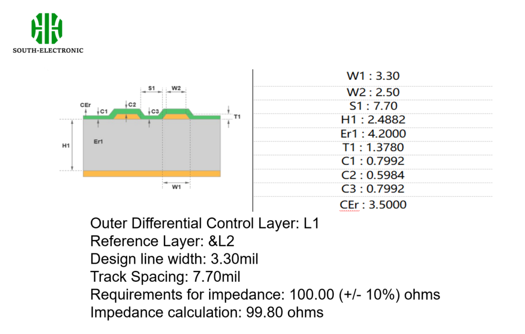
- Differential 100-Ohm Impedance Design on an Outer Layer
Using the DFM tool, select the outer layer single-ended impedance model, enter the corresponding parameters, and calculate the corresponding trace width/spacing to be 3.3/7.7 mils. Since the L1 and L8 layers are symmetrical, the 100-Ohm differential trace width between L1 and L8 is 3.3/7.7 mils, as shown in the figure below.
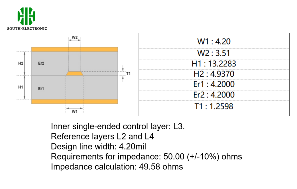
- Inner Layer Single-Ended 50 Ohm Impedance Design
Using the DFM tool, select the outer layer single-ended impedance model, enter the corresponding parameters, and calculate the corresponding trace width to be 4.2 mils. Since the L3 and L6 layers are symmetrical, the 50 Ohm single-ended trace width on the L3 and L6 layers is 4.2 mils, as shown in the figure below.
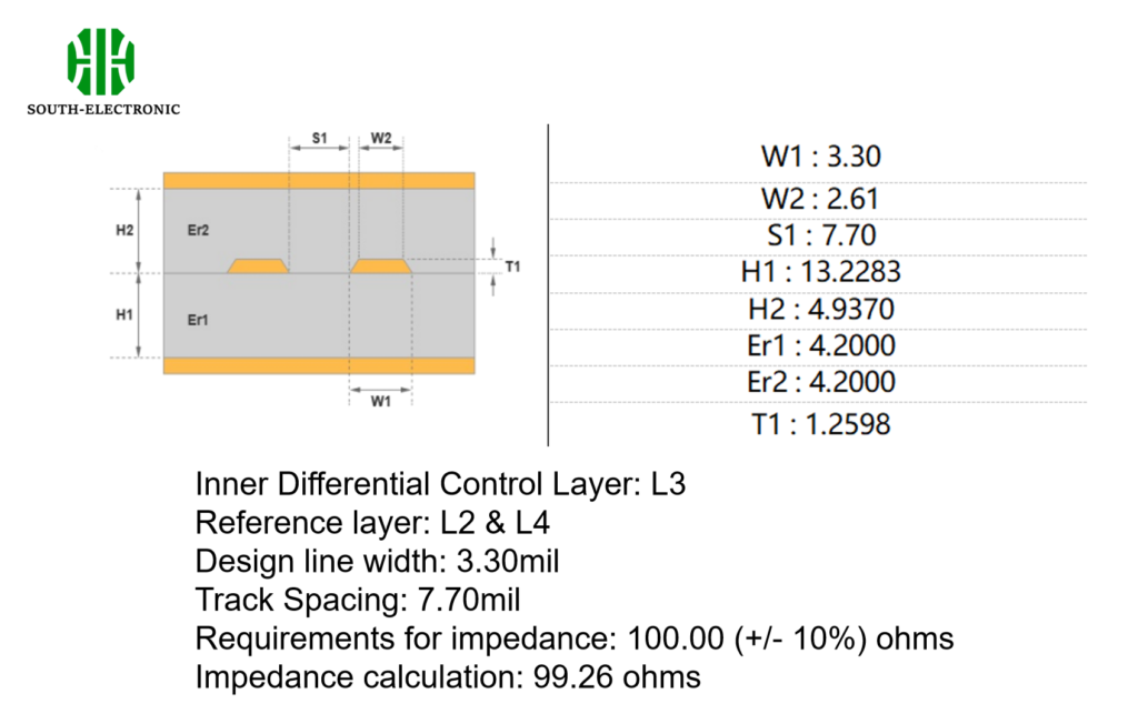
- Inner Layer Differential 100 Ohm Impedance Design
Using the DFM tool, select the outer layer single-ended impedance model, enter the corresponding parameters, and calculate the corresponding trace width/spacing to be 3.3/7.7 mils. Since the L3 and L6 layers are symmetrical, the 100 Ohm differential trace width on the L3 and L6 layers is 3.3/7.7 mils, as shown in the figure below.
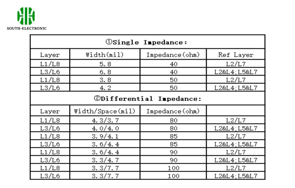
- Overall Impedance and Trace Width