
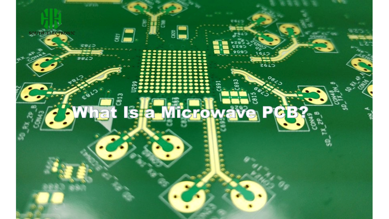
Microwave PCBs can make or break high-frequency electronics. As devices push beyond 1GHz speeds, standard circuit boards struggle with signal loss and interference. What makes these specialized boards the backbone of 5G networks and military radar systems?
Microwave PCBs are high-frequency circuit boards engineered for signals above 1GHz, using materials like PTFE composites and precision manufacturing to minimize signal loss while maintaining impedance control in applications like satellite communications and radar systems.
Traditional circuit boards hit performance walls above 500MHz—but microwave PCBs work higher, faster, and smarter. Let’s explore why these boards aren’t just "better PCBs" but an entirely different class of electronics.
How Do Microwave PCBs Differ From Conventional Circuit Boards?
Your smartphone drops calls in busy areas. Your Wi-Fi slows during peak hours. Why? Conventional PCBs can’t handle high-frequency demands—but microwave boards solve these exact problems.
Microwave PCBs[^1] use low-loss dielectric materials[^2], tighter impedance tolerances (±5% vs ±10%), and specialized plating/etching techniques to maintain signal integrity above 1GHz, unlike standard FR-4 boards optimized for lower frequencies and digital signals.
)
Critical Differences in Design and Performance
| Factor | Microwave PCBs | Conventional PCBs |
|---|---|---|
| Base Material | PTFE, Rogers, Ceramic-filled | FR-4, CEM-3 |
| Dielectric Loss | 0.002-0.004 (tan δ) | 0.02-0.03 (tan δ) |
| Frequency Range | 1GHz-77GHz+ | Up to 500MHz |
| Surface Finish | Electroless Nickel/Gold | HASL, Lead-free HASL |
| Fabrication Cost | 3-8x higher | Baseline |
Microwave boards require material science precision. For example, Rogers 4350B laminate maintains consistent dielectric constant (±0.05) across temperature changes, while FR-4 varies wildly. This stability prevents phase distortion in phased-array antennas. Controlled impedance traces are laser-trimmed to 0.1mm precision versus 0.2mm in standard boards—critical for millimeter-wave 5G bands.
What Materials Are Critical for High-Frequency PCB Performance?
Ever wonder why some circuit boards work flawlessly at 30GHz while others fail at 3GHz? The secret lies in three material properties most engineers overlook.
High-frequency PCBs require materials with stable dielectric constants[^3] (<2% variation), ultra-low dissipation factors[^4] (tan δ <0.005), and copper foils smoother than 0.3µm RMS[^5] to minimize skin effect losses at microwave frequencies.
)
Material Performance Breakdown
| Material | Dielectric Constant (Dk) | Loss Tangent (10GHz) | Thermal Conductivity |
|---|---|---|---|
| Rogers RO4003C | 3.38±0.05 | 0.0027 | 0.6 W/mK |
| PTFE (Generic) | 2.1±0.04 | 0.0009 | 0.25 W/mK |
| FR-4 | 4.5±0.25 | 0.020 | 0.3 W/mK |
| Arlon AD350C | 3.50±0.05 | 0.0035 | 0.6 W/mK |
The 1oz copper’s surface roughness determines signal loss at 28GHz. Standard ED copper (0.5µm RMS) causes 15% more attenuation than low-profile foil (0.2µm RMS). Manufacturers like Isola and Taconic now offer hybrid ceramics—mixing PTFE with SiO2 particles—to balance thermal stability (CTE 15ppm/°C) with machining feasibility.
Which Industries Demand Microwave PCB Technology?
From self-driving cars to fighter jets, microwave PCBs power technologies that seemed impossible ten years ago. But which sectors actually need these expensive, hard-to-machine boards?
Microwave PCBs are mission-critical in telecommunications (5G base stations), aerospace (satellite payloads), defense (phased-array radar), automotive (77GHz collision avoidance), and medical (MRI gradient amplifiers)—applications requiring GHz+ operation with minimal latency and signal distortion.
)
Industry-Specific Requirements
| Sector | Frequency Needs | Key Challenges | Common Materials |
|---|---|---|---|
| 5G Infrastructure[^6] | 24-47GHz | Wide bandwidth + thermal cycling | Rogers RO4835™ LoPro |
| Space Systems | Ku-band (12-18GHz) | Radiation hardness, vibration | Arlon 85N, Cu-clad Invar |
| Automotive Radar | 76-81GHz | Moisture resistance, small form | Isola Astra MT77 |
| Military EW | 0.5-40GHz | EMI shielding, rapid freq hopping | Taconic RF-35A2+ |
In 5G mMIMO arrays, microwave PCBs must handle 64+ antenna elements on a single board while dissipating 200W+ heat—forcing designers to use metal-backed PTFE composites like Taconics TLY-5A. Automotive radars adopt hybrid PTFE-ceramic boards to survive -40°C to 125°C engine bay temps without delamination.
Conclusion
Microwave PCBs enable high-frequency tech by combining specialized materials and precision engineering. They outperform standard boards in speed/thermal stability, powering critical systems from 5G networks to advanced defense radars.
[^1]: Explore this link to understand how Microwave PCBs are revolutionizing high-frequency electronics and their critical role in modern technology.
[^2]: Discover the importance of low-loss dielectric materials in enhancing signal integrity and performance in high-frequency applications.
[^3]: Understanding stable dielectric constants is crucial for optimizing PCB performance at high frequencies. Explore this link for in-depth insights.
[^4]: Ultra-low dissipation factors are key to reducing signal loss in high-frequency applications. Discover more about their significance here.
[^5]: Smoother copper foils minimize skin effect losses, enhancing PCB performance. Learn more about this critical aspect in the linked resource.
[^6]: Discover the critical role of Microwave PCBs in 5G Infrastructure and their impact on communication technology.


