
Custom Multilayer PCB Manufacturing Services
Min trace 3/3 mil | ENIG / HASL | FR-4 & High-TG | AOI & E-Test
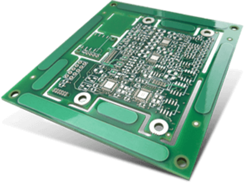
We manufacture high-precision multilayer PCBs for a wide range of applications, including telecommunications, automotive, and consumer electronics. Our focus on quality ensures stable performance and reliability, making us the trusted partner for repeat production.
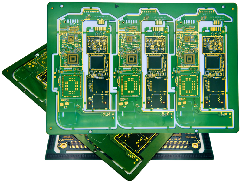
Multilayer PCB Capabilities
Multilayer PCB Process Capability
-
Layer Count
2 to 68 layers
-
PCB Dimensions
≤24*48inch(610*1220mm)
-
Materials Types
FR-4 | High Tg | Halogen-free | PTFE | Ceramic PCB | Metal substrate material
-
Material Brand
Lianmao|Shengyi| Taiyao| Nanya, Panasonic|Isola|Nelco|Rogers|Taconic|Arlon...
-
Board Thickness
0.2mm-8.0mm
-
Finish Treatment
Immersion Gold|Lead-free HASL|OSP|Immersion Tin|Immersion Silver|Thick Gold Plating|Silver Plating|Immersion Gold+OSP
-
Copper thickness
0.33 OZ-8 OZ
-
SolderMask Color
Green| Blue| Black|Yellow| Red|Purple| White...
-
Finish Treatment
Immersion Gold|Lead-free HASL|OSP|Immersion Tin|Immersion Silver|Thick Gold Plating|Silver Plating|Immersion Gold+OSP
Why Choose Us for Multilayer PCB Manufacturing
We provide engineers with reliable multilayer PCB manufacturing,
from prototype builds to stable repeat production.
Every multilayer PCB undergoes a thorough review by our engineers to ensure optimal stack-up, impedance control, and manufacturability before production.
We prioritize consistent quality across all batches, supporting both initial prototypes and long-term production needs.
Skilled in managing tight trace/space requirements, controlled impedance, and multilayer lamination for intricate PCB designs.
We offer clear technical communication and prompt responses to support overseas engineering and purchasing teams effectively.
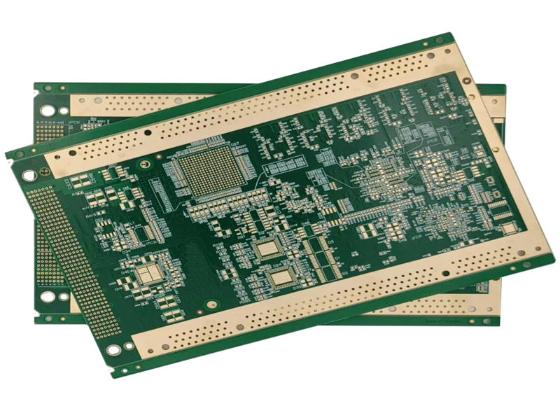
Related Project We Had Done
Multilayer PCB for Industrial Control System
Application
Industrial Control
Key Specs
Challenge
Result
Multilayer PCB for Automotive Power
Application
Key Specs
Challenge
Result
Multilayer PCB for Telecom Equipment
Application
Key Specs
Challenge
Result
Quality Control & Certifications for Multilayer PCB Production
Common Questions
Most Popular Questions
How many layers can a multilayer PCB have?
Multilayer PCBs can range from just 2 layers up to 68 layers, depending on the application’s complexity and requirements.
What materials are commonly used in multilayer PCBs?
Common materials include FR-4, high-TG materials, PTFE, halogen-free laminates, and metal substrates, selected based on the project specifications.
How do you ensure the quality of multilayer PCBs?
We implement a robust quality control process that includes engineering reviews, continuous monitoring during production, and compliance with IPC-A-610 Class 2/3 standards.
What types of finishes are available for multilayer PCBs?
Common finish options include immersion gold, lead-free HASL, OSP, immersion tin, and silver plating, catering to different performance and environmental requirements.
Can you handle high-density designs in multilayer PCBs?
The typical lead time for prototypes is 7–10 working days. For mass production, the lead time varies based on quantity and specifications.
Send Us a Message
The more detailed you fill out, the faster we can move to the next step.
