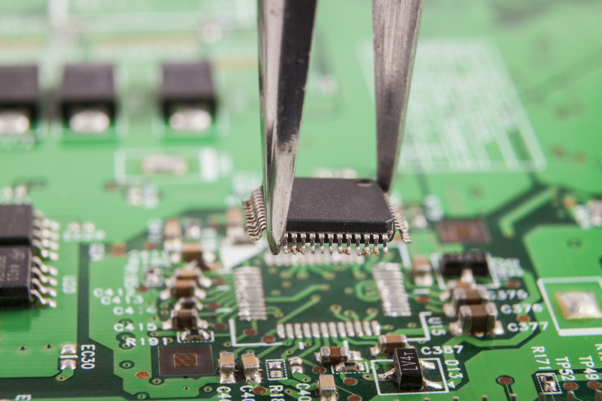
Multilayer PCB Design
South-Electronic
South-Electronic one-stop service seamlessly takes your project from concept to reality, ensuring top performance and durability at every stage. With over a decade of experience, our expert team offers tailor-made solutions to meet the most complex demands, all at competitive prices. Enjoy fast delivery, 24/7 support, and lifetime after-sales service. Trust South-Electronic to elevate your electronic devices to new heights of success!
Why Choose South-Electronic?
You can trust South-Electronic to deliver unmatched quality, reliability, and exceptional value.
With our one-stop multilayer PCB design service, you’ll experience a seamless journey from concept to completion. We guarantee precision, durability, and strict adherence to industry standards, ensuring your satisfaction every step of the way.
-
Customized Design
Customized Design to Meet Your Unique Needs.
At South-Electronic, we understand that every project is unique. That's why our PCB layout services are customized to meet your specific requirements, ensuring that every detail is executed to your exact specifications. This will improve the performance and reliability of your products. -
Guaranteed Satisfaction
You’ll appreciate the confidence that comes with working with an ISO9001 certified company.
We prioritize clear, transparent communication and hold ourselves to the highest standards, ensuring that your Multilayer PCBs not only meet but exceed your expectations for performance, durability, and precision. -
One-Stop Service
When you choose us, you get a complete PCB solution from design and prototyping to mass production.
We offer a one-stop service, eliminating the complexity and cost of dealing with multiple suppliers. -
Comprehensive Service
You get complete satisfaction with our wide range of equipment.
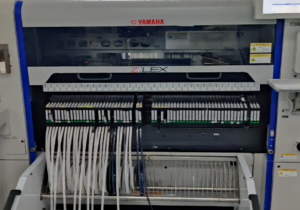
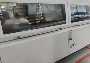
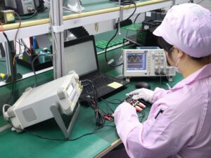
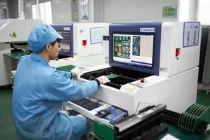
We have a wide range of PCB processing capabilities. From design to delivery, we have the equipment and processes to make sure your order is done right. -
Fast Delivery
You stay on schedule with our fast turnaround times.
Our streamlined production ensures fast turnaround times, so you get your products when you need them, without delays.
Related Project We had Done
Customer Reviews
Common Questions
Most Popular Questions
Send us a message
The more detailed you fill out, the faster we can move to the next step.












The Complete Guide For Multilayer PCB Design
Contents
Chapter 1

Introduction to Multilayer PCBs
What Are Multilayer PCBs and Why Are They Important?
A Multilayer PCB (Printed Circuit Board) is a complex type of circuit board that consists of multiple layers of electrical components sandwiched between layers of insulating material. Unlike traditional single-layer PCBs, which have components on only one side of the board, multilayer PCBs stack multiple layers on top of each other, with each layer separated by insulation. This design allows for more components to be packed into a smaller space, increasing the functionality and efficiency of the device.
The Transition from Single-Layer PCBs
The transition from single-layer to multilayer PCBs represents a major advancement in electronic design technology. In the early days of electronics, single-layer PCBs were sufficient for the needs of early electronic devices. However, as technology progressed, the demand for smaller, higher-speed devices increased. This led to the development of double-layer, and eventually, multilayer PCBs.
Each additional layer allows for a higher density of components and interconnections that are not possible with single-layer designs. This transition has enabled the creation of increasingly complex and powerful electronics.
Overview of Components and Functionality
The main components of a multilayer PCB include:
- Conductive Pathways (Traces):
These are thin lines of copper or another conductive material that are etched onto the board and serve as the circuit’s wiring.
- Dielectric Layers:
These insulating layers separate the conductive copper layers and prevent electrical shorts between different layers.
- Vias:
These are small holes drilled into the PCB that allow electrical connections between different layers. Vias can be through-hole, blind, or buried, depending on whether they connect all layers or only specific ones.
Pads:
These are exposed areas of metal where components are soldered.
In terms of functionality, multilayer PCBs offer several advantages over single-layer PCBs:
- Higher Capacity and Density: They can support more circuits per unit area, essential for modern, compact devices.
- Improved Durability: The multilayer design offers greater protection against environmental factors like heat and moisture.
- Enhanced Performance: The arrangement of multiple layers can reduce electromagnetic interference (EMI) and signal losses, crucial for maintaining the integrity of high-speed signals.
Multilayer PCBs have changed the way we design electronics by allowing us to keep up with technology while making things smaller. They let us put a lot of complex circuitry into a small space, and they make things work better and last longer. That’s why you see them in everything these days.
Chapter 2
Why You Should Use Multilayer PCBs
More Functionality in a Smaller Space
One of the biggest advantages of multilayer PCBs is that they allow you to get more functionality into a smaller space. This is a huge deal in industries where space is at a premium. By stacking multiple layers, these PCBs make room for more components and interconnections. That means you can pack more functionality into smaller devices, like smartphones, smartwatches, and medical implants, where traditional single-layer PCBs just wouldn’t cut it.
Better Durability and Reliability
When you choose a multilayer PCB, you’re getting a more durable product. The multiple layers of materials in these PCBs include high-quality insulators that protect the conductive copper layers. This structure not only guards against environmental threats like moisture and thermal stress but also provides mechanical stability. The result is a product that stands up better over time, making multilayer PCBs ideal for applications in harsh environments, such as automotive electronics, military equipment, and outdoor telecommunications hardware.
Better Performance with Less Electromagnetic Interference (EMI)
With multilayer PCBs, you can get better performance, especially in terms of signal integrity. These PCBs are designed to have internal power and ground layers that shield the signal-carrying layers, which significantly reduces electromagnetic interference (EMI). This makes them perfect for high-speed circuits where maintaining signal integrity is critical. You’ll notice this improvement in applications like data centers, high-speed routers, and advanced computing systems where even a little interference can lead to data errors.
Critical for Modern Compact and High-Density Devices
The benefits of multilayer PCBs are especially critical in modern electronics that are not only expected to perform multiple functions but also to fit into increasingly smaller spaces. Think of your latest smartphone or a cutting-edge drone—these devices require dense component configurations that only multilayer PCBs can support efficiently. Moreover, the design flexibility offered by multilayer PCBs allows for optimal component placement, which leads to better connectivity and shorter transmission paths, improving the overall device performance.
Used in a Wide Range of Industries
Multilayer PCBs are used in a wide range of industries, including healthcare, consumer electronics, automotive, and aerospace. In each of these fields, the small size, durability, and performance of multilayer PCBs provide the technology needed to drive innovation. Whether it’s wearable tech that monitors your health, eco-friendly smart cars, or aerospace electronics, multilayer PCBs are at the heart of advancements that push the boundaries of what technology can do.
When you use multilayer PCBs in your designs, you’re not just keeping up with the current trends in technology; you’re setting the stage for future innovations. With all their benefits, these PCBs not only meet today’s high standards but also anticipate tomorrow’s challenges, making them a key part of the evolution of electronic devices.
Chapter 3
Key Design Considerations for Multilayer PCBs
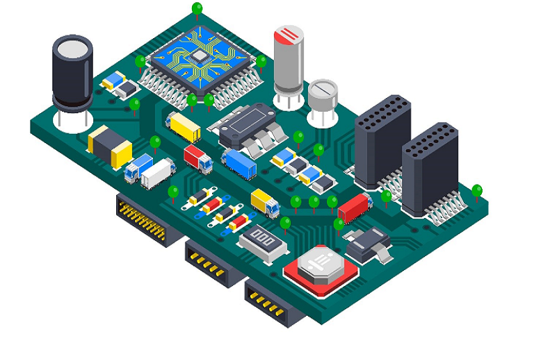
Designing a multilayer PCB is a lot more complicated than designing a single-layer board. Here are some things you need to think about to make sure your multilayer PCB works properly and is reliable.
Choose the Right Material
Choosing the right material is really important when you’re designing a multilayer PCB. The material affects everything from how durable your board is to how well it conducts electricity. The most common material is called FR-4, which is a fiberglass and epoxy laminate. It’s popular because it’s a good balance between cost and performance. If you’re working on a high-frequency application, you might need to use a more advanced material like Rogers or Teflon, which have lower dielectric losses.
The material you choose affects how well your PCB can handle heat, how strong it is, and how well it conducts electricity. For example, materials with a low coefficient of thermal expansion (CTE) are better at managing heat and are less likely to have mechanical problems when the temperature changes. This is especially important in high-density or high-power devices where heat is a big issue.
Decide How Many Layers You Need
Deciding how many layers your PCB needs is a big deal because it affects how much your board costs and what it can do. More layers let you pack more stuff into your board and make more complicated circuits, which is important for high-performance electronics. But every layer you add makes your board more expensive and harder to manufacture.
When you’re deciding how many layers your board needs, think about how important it is for your signals to work right and how much electricity your board needs. If you’re working on something with really fast signals, you might need to have special layers in your board just for power and ground to make sure everything works right and to keep the signals from messing with each other.
Trace Width: Ensuring Signal Integrity and Power Handling
The width of the lines on your board is really important because it affects how much current your board can handle without getting too hot and how well your signals work. Thinner lines let you fit more stuff in a smaller space, but they might not be able to handle as much current, which can make them get hot and maybe even break.
The width of the lines is also really important for making sure the impedance is right, especially if you’re working on something with really fast signals. You need to make sure the impedance is right so your signals don’t bounce back and forth and get all messed up. There are software tools that can help you figure out the right line width based on how much current you need and what impedance you need for your specific project.
Addressing Electromagnetic Interference (EMI) and Crosstalk
When you’re designing a multilayer PCB, it’s really important to think about how you’re going to keep the signals from messing with each other and how you’re going to keep noise from getting into your signals. One way to do this is to put power and ground planes in your board in the right places. This can help keep the signals from getting messed up by noise. You also need to think about how you’re going to route your signals. One thing you can do is use differential signaling, which can help keep noise from getting into your signals. You also need to make sure you have enough space between your traces so they don’t mess with each other.
Via Design: Connecting Your Layers Effectively
Vias are another really important part of designing a multilayer PCB. You have to decide if you want to use through-hole vias, blind vias, or buried vias, depending on what you’re trying to do and how much money you have. Through-hole vias are the cheapest and easiest to make, but they take up a lot of space. Blind and buried vias let you save space and make your board work better, but they make it harder and more expensive to make your board.
If you think about all of these things—what material you’re going to use, how many layers you need, how wide your lines are, how you’re going to keep noise out of your signals, and what kind of vias you’re going to use—you can make your multilayer PCB work really well and not cost too much. These decisions don’t just affect how your board works, but they also affect how much it costs and how easy it is to make. When you’re working on your next PCB, think about all of these things to make sure you design a good board that’s easy to make.
Chapter 4
Step-by-Step Design Process for Multilayer PCBs
Designing a multi-layer PCB is a systematic activity that needs to be gently executed. No matter if you are a professional PCB designer or just starting your journey, following a structured approach will guarantee the functionality and reliability of your final product. Follow these steps and you will be successful in designing your first multi-layer PCB.
Step 1: Idea and Requirement Analysis
Before you start designing your PCB, you must be clear about what you want to achieve and what your PCB needs to do. What is the purpose of the PCB? What are the environmental conditions that the PCB will be exposed to? Knowing the answers to these questions will help you decide what materials to use, what components to choose, and how many layers and connections you will need. Make a list of all the components you plan to use and gather their datasheets for reference.
Step 2: Schematic Design
Using a PCB design tool, start by creating the schematic of your circuit. This involves drawing a diagram that shows all the components and how they are connected. It is very important to double-check each connection for accuracy at this stage because mistakes here can cause big problems later on. Tools like OrCAD, Altium Designer, or Eagle can be used for schematic design. These tools provide a visual representation that helps you make sure everything is in the right place and makes sense.
Step 3: Layer Stackup Planning
After you have finished your schematic, you need to plan your layer stackup. This means deciding how many layers your PCB will have and what each layer will do. Common configurations include signal layers, power planes, and ground planes. The goal is to minimize signal integrity problems and manage electromagnetic interference (EMI). For high-speed circuits, consider placing ground planes next to signal layers to provide shielding and impedance control.
Step 4: Layout Design
Move from the schematic to the layout design in your PCB software. Here, you will place components and route traces between them based on the connections you defined in the schematic. Pay close attention to the placement of critical components to minimize the length of traces, which will reduce delay and interference. Use automatic routing tools with manual adjustments to optimize routing paths and make sure traces are wide enough to carry current and meet impedance requirements.
Step 5: Verification and Signal Integrity Checks
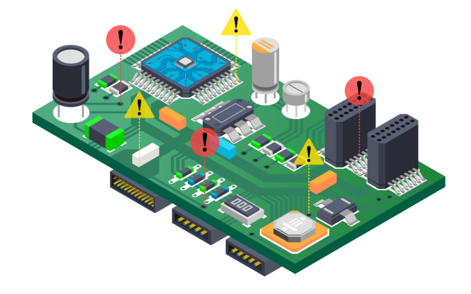
After you have finished your layout, you need to make sure that everything meets the requirements. Use the tools in your PCB design software to check for errors like traces crossing each other, not enough space between traces and components, and other potential problems. Do signal integrity analysis to make sure that all signals will be transmitted with minimal loss and interference. This step may require several iterations to fine-tune the layout for optimal performance.
Step 6: Prototype Manufacturing
Once you have verified your design, you are ready to make a prototype. This will allow you to test your PCB in real-world conditions and find any functional or performance problems. Choose a reliable PCB manufacturer and give them your design files, usually in Gerber format, which contains all the data they need to make your PCB.
Step 7: Testing and Iteration
Test your prototype in conditions that are similar to the conditions in which it will be used. Look for functionality and any differences in performance. If you find any problems, go back to your design and make the necessary changes. This might mean going back to any of the previous steps, from changing the schematic to changing the layout or even changing the stackup.
Step 8: Final Production
After you have tested your prototype and made any necessary changes, your PCB design is ready for production. This means scaling up the manufacturing process to make as many PCBs as you need, and making sure that each batch is made to the same quality standards as the prototype.
If you follow these steps carefully, you will be able to design and make a high-quality multi-layer PCB that does what you want it to do and works reliably in the real world. Each step is important and requires careful thought to make sure that your electronic product is a success.
Chapter 5
Strategies for Creating an Effective Layer Stackup for Multilayer PCBs
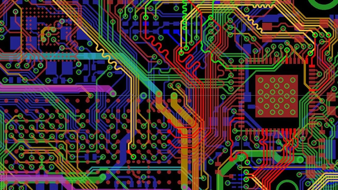
When you design the layer stackup for your multi-layer PCB, it’s like laying the foundation for a building its critical to the stability, functionality, and integrity of your board. In this post, we’ll dive into the strategies for creating an effective layer stackup, with a focus on improving both signal and power integrity.
Understanding the Layer Stackup
The layer stackup is how the different layers (signal, power, and ground) are arranged in a multi-layer PCB. This arrangement affects the electrical performance of the board, as well as manufacturability and cost. An optimal stackup helps minimize signal integrity issues, manage electromagnetic interference (EMI), and ensure robust power distribution.
Strategy 1: Focus on Signal Integrity
To maintain signal integrity, your stackup should minimize the distance signals have to travel between components, reducing the chances of signal loss and cross-talk. Here’s how you can do it:
Pair Adjacent Layers:Put signal layers next to either ground or power planes. This will shield the signal layers and give the signal a return path, reducing cross-talk and EMI.
Symmetry and Balance:
Aim to keep your stackup symmetrical to prevent the board from warping during manufacturing. A symmetrical stackup also ensures consistent electrical characteristics of the board.
Strategy 2:Nail Down Power Integrity
Power integrity is all about maintaining a stable, clean power distribution across the board. To do this, you need to strategically place your power and ground layers:
- Dedicated Power and Ground Planes:
Use dedicated layers for power and ground. This will lower the impedance of your power distribution network and help you effectively spread the current load, which is critical for high-power applications.
Keep Power and Ground Layers Close:When you place your power and ground planes close to each other, you can reduce the overall inductance.
Strategy 3: Minimize EMI and Thermal Issues
Effective layer stackup can also help in minimizing EMI and managing thermal performance:
Interleave Ground Planes: Use multiple ground layers interleaved between signal layers. This setup acts as a shield against EMI and helps in heat dissipation, especially important in high-speed or high-frequency applications.
Thermal Vias: Incorporate thermal vias in the stackup to help transfer heat from hot components to a heat sink or external environment, preventing overheating.
Strategy 4:Consider HDI (High Density Interconnect) Technologies
For really complex or compact designs, you might want to consider using High Density Interconnect (HDI) technologies. HDI boards have finer spaces and lines, smaller vias, and higher connection pad densities than traditional PCBs:
Microvias: Use microvias to connect only the layers that need to be connected, saving space and improving the integrity of high-speed signals.
Stacked Vias: Use stacked vias in dense component areas to maximize space and improve connectivity between layers.
Finalize Your Stackup
Once you’ve planned your layer stackup using these strategies, review it with your PCB manufacturer. They can provide valuable input, especially when it comes to manufacturability and cost implications. They can also give you insights on the latest materials and technologies that could further optimize your design.
Remember, the layer stackup you choose directly impacts the performance and reliability of your multilayer PCB. By carefully planning your stackup strategy, you ensure that your board meets all the necessary electrical standards and performs reliably in its intended application.
Chapter 6
Signal integrity and impedance control in Multilayer PCBs
Signal integrity and impedance control are two of the most important aspects of multilayer PCB design, especially when dealing with high-speed electronic circuits. In this article, we will explain why these two elements are so critical and how you can effectively manage them to ensure your PCB performs at its best.
What is signal integrity?
Signal integrity refers to the condition in which digital and analog signals are transmitted without significant degradation. In multilayer PCBs, maintaining signal integrity is crucial because any distortion or loss can lead to data errors, system instability, and decreased performance. As your PCBs handle faster signals and higher frequencies, the challenges related to signal integrity escalate, making meticulous design and control imperative.
The role of impedance control
Impedance is the measure of opposition that a circuit presents to a current when a voltage is applied. In PCB design, controlling impedance involves ensuring that the impedance of the PCB traces matches the source and load impedances. This matching is crucial for preventing signal reflections and losses, which can occur if there are impedance mismatches along the signal path.
Here’s how you can ensure effective impedance control and maintain signal integrity:
Strategy 1: Use controlled impedance traces
Trace width and spacing: Determine the appropriate trace width and spacing based on the dielectric material and the thickness of the PCB. Use PCB design software to calculate the optimal dimensions that will achieve the desired impedance.
Consistent trace geometry: Maintain consistent trace geometry throughout the circuit to avoid impedance discontinuities. Variations in trace width, thickness, or dielectric constant can lead to impedance mismatches and signal reflections.
Strategy 2: Optimize the PCB layer stackup
- Symmetrical Stackup: Design a symmetrical stackup where possible, as this helps in balancing the capacitance and inductance across the PCB, leading to more stable impedance characteristics.
- Adjacent Ground and Power Planes: Place ground and power planes adjacent to signal layers to provide shielding and reduce the loop area, minimizing inductive coupling and enhancing signal integrity.
Strategy 3: Minimize Cross-Talk
- Proper Trace Routing: Route parallel traces as far apart as possible or use ground traces between them to reduce capacitive coupling. Consider using differential signaling for critical high-speed lines, as it is less susceptible to noise and electromagnetic interference.
- Avoid Right-Angle Bends: Right-angle bends in traces can cause impedance changes and signal reflection. Use smoother transitions such as 45-degree angles or curved bends to maintain consistent impedance.
Strategy 4: Manage Signal Pathways
- Shorter Trace Lengths: Keep the trace lengths as short as possible to reduce the chances of signal degradation over distance. This is particularly important for high-frequency signals where longer traces can lead to significant losses.
- Via Design: Use vias carefully as they can introduce impedance discontinuities. Opt for back-drilled or blind/buried vias in high-frequency applications to reduce the stub length and minimize reflections.
Testing and Verification
Once your design is complete, it’s essential to test and verify the signal integrity and impedance control:
- TDR (Time Domain Reflectometry) Testing: Use TDR testing to measure the impedance profile along the traces and identify any discrepancies or mismatches.
- Simulation Tools: Utilize simulation software to model and analyze the signal integrity before the physical PCB is manufactured. This helps in identifying potential issues early in the design process.
By focusing on these strategies, you ensure that your multilayer PCB will handle high-speed signals efficiently, with minimized risk of data corruption or loss. Effective impedance control and signal integrity management are not just about following guidelines—they’re about understanding the physics behind your PCB’s operation and making informed decisions to optimize its performance and reliability.
Chapter 7

Thermal Management in Multilayer PCBs
Effective thermal management is a crucial aspect of multilayer PCB design, especially as devices become more compact and power densities increase. Here’s a guide on how you can navigate the challenges of heat management in your PCB designs and ensure that your devices operate reliably without overheating.
The Challenges of Heat Management in Multilayer PCBs
As multilayer PCBs pack more components into smaller areas, the generated heat can become concentrated, leading to higher temperatures. This increase in temperature can affect the performance, reliability, and lifespan of electronic components. Managing this heat effectively is crucial, particularly in high-power applications like LED lighting systems, power converters, and computer processors, where excess heat can lead to failure.
Techniques for Effective Heat Dissipation
Here are several strategies and techniques you can use to enhance thermal management in your multilayer PCBs:
1. Thermal Vias
One of the most effective ways to manage heat in multilayer PCBs is through the use of thermal vias. These are special vias designed to create a thermal path from heat-producing components to a heat sink or other cooling mechanism.
- Via Placement: Place thermal vias directly under or very close to heat-generating components to help conduct heat away from these components efficiently.
- Via Design: Opt for larger diameter vias and higher via density to improve the thermal conductivity. Filling the vias with a conductive material can also enhance their ability to transfer heat.
2. Material Selection
The choice of materials used in your PCB can significantly affect its thermal management capabilities.
- Thermal Conductivity: Select materials with higher thermal conductivity for the substrate, such as ceramic-based materials or high thermal conductivity FR-4, to help spread out heat more evenly across the board.
- Metal Core PCBs: Consider using metal core PCBs (MCPCBs) for extremely high-power applications. These PCBs incorporate a metal layer (typically aluminum or copper) that serves as an excellent heat spreader.
3. Layer Stackup Configuration
The way you configure the layers in your PCB can influence its ability to dissipate heat.
- Heat Dissipation Layers: Integrate dedicated layers that can act as heat spreaders within the stackup, especially near the top and bottom layers where heat can be transferred to the environment or to heat sinks more easily.
- Ground and Power Planes: Utilize copper planes for power and ground as they can also serve as excellent heat spreaders due to their high thermal conductivity.
4. Component Placement and Layout
How components are placed and how the board is laid out can also impact thermal management.
- Avoid Heat Concentration: Space out power-intensive components to avoid creating hot spots on the PCB.
- Thermal Relief: Ensure that heat-sensitive components are placed in areas with good ventilation or near cooling mechanisms.
5. Heat Sinks and Cooling Solutions
In addition to PCB design considerations, external cooling solutions can be crucial.
- Heat Sinks: Attach heat sinks directly to heat-generating components or to the PCB itself if large areas generate heat.
- Active Cooling: Implement fans or liquid cooling systems in scenarios where passive cooling isn’t sufficient to manage the heat.
Testing and Verification
Finally, it’s important to test your PCB under realistic operational conditions to see how well it manages heat. Thermal cameras and sensors can help you detect hot spots and verify the effectiveness of your thermal management strategies.
By implementing these techniques, you can ensure that your multilayer PCBs operate reliably and efficiently, even under high thermal loads. Effective thermal management not only extends the lifespan of your products but also enhances their performance and safety.
Chapter 8
Common Mistakes and How to Avoid Them
Designing multilayer PCBs can be a complex task filled with potential pitfalls that could compromise the performance and reliability of your electronics. Being aware of these common issues and knowing how to avoid them will help ensure a smoother design process and a more robust final product. Here’s a guide on the typical challenges you might face and the best practices to circumvent them.
Pitfall 1: Inadequate Planning for Signal Integrity
Problem: Failing to properly plan for signal integrity can lead to issues like signal loss, cross-talk, and electromagnetic interference (EMI), which are particularly critical in high-speed circuits. Solution: Always plan your layer stackup with signal integrity in mind. Use ground planes adjacent to signal layers to provide shielding and maintain impedance control. Consider using differential pairs for critical signals and ensure that trace lengths are minimized and matched for critical signal paths.
Pitfall 2: Poor Thermal Management
Problem: Multilayer PCBs often suffer from inadequate thermal management, leading to overheating and reduced component lifespan. Solution: Use thermal vias strategically placed under or around heat-generating components to facilitate heat transfer to a heat sink or the outer layers. Select materials with higher thermal conductivity for layers near heat sources and consider the incorporation of a metal core layer if extreme heat is expected. Also, ensure proper spacing between high-power components to avoid hot spots.
Pitfall 3: Incorrect Via Use
Problem: Incorrectly placed or poorly designed vias can cause a variety of issues, including broken connections and impedance discontinuities. Solution: Plan your via placement carefully to minimize the path electrical signals must travel, reducing latency and signal degradation. Use blind or buried vias to save space and reduce layer-to-layer connections when not every layer needs to be interconnected. Ensure that vias are properly sized to handle the current load and that they do not compromise the structural integrity of the board.
Pitfall 4: Cross-Talk Between Traces
Problem: Cross-talk is a frequent issue in densely packed multilayer PCBs, where the electromagnetic field of one trace affects another, leading to unwanted interference. Solution: Increase the distance between parallel traces or place a ground plane between them to reduce capacitive and inductive coupling. Route critical traces perpendicularly to each other if they must cross, and consider using shielded traces for highly sensitive signals.
Pitfall 5: Component Misplacement
Problem: Improper placement of components can lead to issues like difficulty in routing, electromagnetic interference, and thermal imbalances. Solution: Group similar components together to minimize the length of critical connections and use simulation tools to check for electromagnetic compatibility (EMC) issues. Keep sensitive components away from high-frequency or high-power components and ensure that there is enough space for heat dissipation.
Pitfall 6: Overlooking Manufacturing Constraints
Problem: Designing without considering the manufacturing capabilities can lead to a PCB that is either too expensive or impossible to produce. Solution: Engage with your PCB manufacturer early in the design process to understand their capabilities and limitations. Design according to their specifications for trace widths, spacing, and via dimensions to ensure manufacturability and to keep costs in control.
Pitfall 7: Insufficient Testing and Verification
Problem: Skipping comprehensive testing phases can lead to undetected issues cropping up in the final product. Solution: Implement a rigorous testing protocol that includes both software simulations for electrical performance and physical testing for thermal and mechanical reliability. Use tools like Time Domain Reflectometry (TDR) for impedance analysis and thermal imaging to detect hot spots and thermal performance.
By being mindful of these common pitfalls and implementing the suggested solutions, you can significantly enhance the quality and reliability of your multilayer PCB designs. This proactive approach not only improves the functionality of your product but also reduces the risk of costly revisions and redesigns.
Chapter 9
Testing and Fixing Problems in Multilayer PCBs
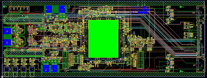
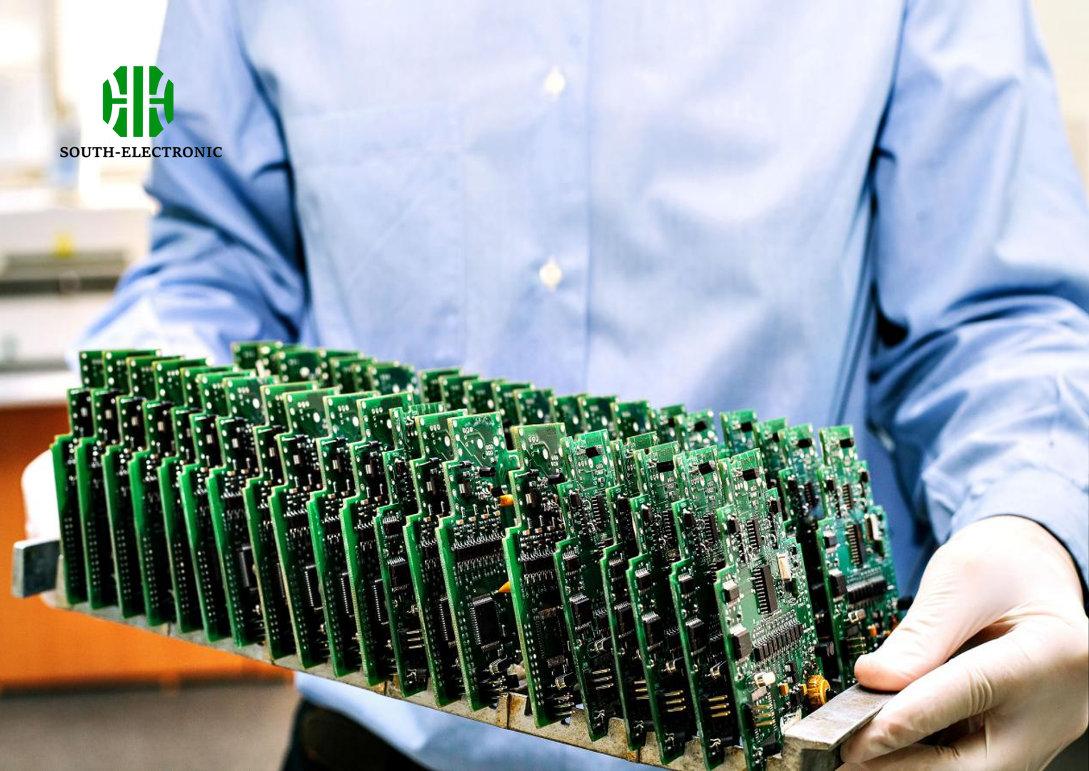
Ensuring the functionality and reliability of your multilayer PCBs requires thorough testing and efficient troubleshooting. Here’s how you can methodically test your PCBs and effectively troubleshoot common issues, ensuring your product meets both performance standards and durability requirements.
Testing Multilayer PCBs
1. Electrical Testing:
- Continuity Testing: This should be your first step. It verifies that all connections on the PCB are correctly made and that there are no short circuits. Use a multimeter or an automated test equipment (ATE) that checks each connection point against the PCB design files.
- In-Circuit Testing (ICT): ICT is more comprehensive, checking for shorts, opens, resistance, capacitance, and other electrical parameters that can affect the functionality of the PCB. It requires physical access to all nodes, so plan for test points in your design.
2. Functional Testing:
- Power-On Test: Apply power to the PCB and monitor the initial responses. Check for expected voltages at various points and observe any unexpected behavior like resets or failure to start.
- Signal Integrity Test: Use oscilloscopes and logic analyzers to ensure that high-speed signals are clean and free from undue noise and distortion. This test is crucial for circuits involving high-frequency components.
3. Environmental Testing:
- Temperature Cycling: Expose the PCB to various temperatures to ensure it can handle environmental stresses. This helps in identifying potential failures caused by thermal expansion.
- Humidity Testing: Simulate high humidity environments to check for potential failures due to condensation or moisture ingress, which can cause corrosion or short circuits.
Fixing Problems In Common PCB
1. Intermittent Failures:
- These are often due to poor solder joints or hairline fractures in traces. Use a magnifying glass or microscope to inspect solder joints and reflow any suspect joints. Thermal imaging can help identify hot spots that indicate a poor connection.
2. Signal Integrity Issues:
- If you’re experiencing noise, loss, or data corruption, review your trace routing and shielding practices. Consider adding additional shielding or rerouting traces to minimize interference. Re-check your impedance matching and ensure all termination points are correctly implemented.
3. Overheating Components:
- Overheating can be a symptom of excessive current draw or inadequate thermal management. Check that your power distribution network is correctly designed and that all components are rated for the current they are handling. Enhance thermal paths using additional vias or by improving heat sink designs.
4. Power Issues:
- Verify that all power supplies deliver the correct voltages and that power regulation components function within specified limits. Use a current probe to measure the actual power consumption of the board and ensure it matches the expected values.
5. Functional Errors:
- These might occur due to incorrect component placement, wrong component values, or logic errors in the circuit design. Check all components against the schematic for correctness, and re-validate your circuit logic through simulation tools.
Documenting the Process
Keep a detailed log of all tests performed, including conditions, results, and any anomalies observed. This documentation is invaluable for troubleshooting recurring issues and for refining future designs.
Testing and troubleshooting are integral parts of the PCB design lifecycle. By methodically applying these practices, you ensure that your multilayer PCBs are not only functionally robust but also reliable across various operational and environmental conditions. This diligence not only enhances the quality of your product but also its longevity in the field.
Chapter 10
Future Trends in Multilayer PCB Design
As technology continues to advance, so do the techniques and materials used in PCB design. Here’s a glimpse into the future of multilayer PCB design, highlighting innovations that could revolutionize how you approach these complex systems.
1. Flexible and Stretchable PCBs
Imagine PCBs that can bend, flex, and even stretch. Flexible and stretchable PCBs are set to expand the possibilities of electronics design, particularly in wearable technology, medical devices, and even in automotive applications. These PCBs use materials like polyimide or polyester film that allow them to conform to non-traditional surfaces or move without breaking. This adaptability opens up new design opportunities for devices that must operate in dynamic or irregular environments.
2. AI-driven Design Tools
AI and machine learning are transforming how PCBs are designed. AI-driven design tools can automate complex processes such as routing and layout optimization, significantly reducing design time and potential errors. These tools can analyze vast amounts of data to suggest optimal designs based on predefined criteria, such as minimizing noise or reducing material costs. As AI technology progresses, expect these tools to provide even more sophisticated insights, further streamlining the design process.
3. Integration of Advanced Materials
The use of advanced materials in multilayer PCBs is on the rise. Materials like graphene and conductive polymers are being explored for their exceptional electrical, thermal, and mechanical properties. Graphene, for instance, offers excellent electrical conductivity and thermal management capabilities, which could lead to faster, cooler-running boards. As these materials become more accessible, they could dramatically improve the performance and durability of PCBs.
4. 3D Printing of PCBs
3D printing technology is poised to transform PCB manufacturing by enabling rapid prototyping and complex, multi-layer designs that are difficult to achieve with traditional manufacturing methods. 3D printing allows for the direct integration of electronic components into the PCB during the manufacturing process, reducing assembly time and potentially enhancing the reliability of the finished boards.
5. HDI Technology Advancements
High Density Interconnect (HDI) technology, which allows for finer lines and spaces, smaller vias, and denser component placement, is expected to evolve further. Future developments may include even smaller microvias and improved via fill materials, enhancing electrical performance and board reliability. This will be crucial for supporting the ongoing trend towards miniaturization in electronics.
6. Enhanced Thermal Management Solutions
As components become smaller and power densities increase, managing heat in multilayer PCBs becomes even more critical. Future trends include the integration of novel cooling techniques, such as embedded cooling channels or thermally conductive layers that can actively draw heat away from hot spots. Such innovations will be essential for high-performance computing and power electronics.
7. More Robust Simulation and Testing Tools
Expect to see advancements in simulation software that can model electrical, thermal, and mechanical behaviors more accurately. These tools will help designers predict how multilayer PCBs will perform under various conditions before they are physically built, reducing the need for multiple prototypes and helping to ensure that the final product meets all specifications.
By staying informed about these trends, you can better prepare for the future of multilayer PCB design. Whether it’s leveraging new materials, utilizing AI tools, or adopting novel manufacturing techniques, these innovations promise to enhance the capabilities and performance of PCBs, enabling the next generation of electronic devices.
Get in touch
Where Are We?
Industrial Park, No. 438 Donghuan Road, No. 438, Shajing Donghuan Road, Bao'an District, Shenzhen, Guangdong, China
Floor 4, Zhihui Creative Building, No.2005 Xihuan Road, Shajing, Baoan District, Shenzhen, China
ROOM A1-13,FLOOR 3,YEE LIM INDUSTRIAL CENTRE 2-28 KWAI LOK STREET, KWAI CHUNG HK
service@southelectronicpcb.com
Phone : +86 400 878 3488
Send us a message
The more detailed you fill out, the faster we can move to the next step.


