
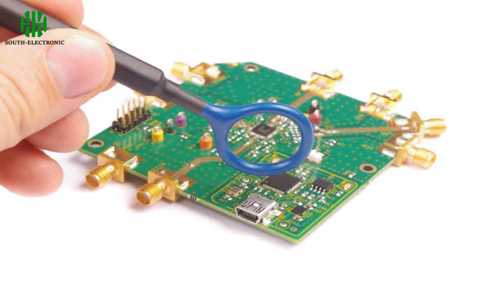
Optimizing a PCB (Printed Circuit Board) design is crucial for ensuring performance, reliability, and manufacturability. Here are eight essential tips to help you achieve an optimized PCB.
内容
隐藏
The Best Practices for Component Placement
- Group Related Components: Place components that are electrically connected or functionally related close to each other to minimize trace lengths and reduce noise.
- Keep High-Speed Signals Short: Ensure high-speed signal paths are as short as possible to reduce delay and potential interference.
- Optimize Layout for Heat Dissipation: Place heat-generating components, such as power regulators and microcontrollers, in areas where heat sinks or thermal vias can be effectively used.
- Avoid Crosstalk: Place sensitive analog components away from high-speed digital components to prevent crosstalk and interference.
- Ensure Accessibility: Arrange components to allow easy access for testing, rework, and repair.

Reduce Signal Interference
- Use Ground Planes: Implement a continuous ground plane to provide a low-impedance path for return currents and shield against interference.
- Minimize Loop Areas: Reduce the loop area of signal and return paths to minimize inductive coupling and interference.
- Shield Sensitive Signals: Use shielding techniques, such as ground shielding or guard traces, to protect sensitive signals from interference.
- Isolate High-Frequency Components: Separate high-frequency components from low-frequency analog signals to reduce noise coupling.
Improve the Thermal Management
- Use Thermal Vias: Place thermal vias around heat-generating components to dissipate heat through the board layers.
- Implement Heat Sinks: Attach heat sinks to high-power components to enhance heat dissipation.
- Optimize Component Placement: Position heat-sensitive components away from heat sources and ensure adequate airflow around hot spots.
- Choose Thermal Conductive Materials: Use materials with high thermal conductivity for the PCB substrate and copper layers.

Ensure Proper Grounding in PCB Design
- Use a Ground Plane: A solid ground plane provides a low-impedance path for return currents and reduces EMI.
- Star Grounding: Implement star grounding to ensure all ground connections converge at a single point, minimizing ground loops.
- Minimize Ground Impedance: Use wide ground traces and multiple ground vias to reduce ground impedance.
- Separate Analog and Digital Grounds: Keep analog and digital grounds separate to prevent noise from digital circuits affecting analog signals.

Reduce Electromagnetic Interference (EMI)
- Shielding: Use metal enclosures or EMI shields around sensitive components and circuits.
- Filtering: Implement EMI filters, such as ferrite beads and capacitors, to suppress unwanted high-frequency noise.
- Ground Planes and Power Planes: Use continuous ground and power planes to reduce EMI by providing low-impedance paths.
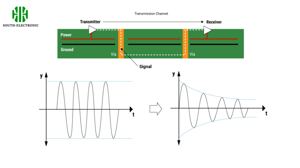
- Proper Trace Routing: Route high-speed signals carefully to avoid parallel runs and reduce radiation.

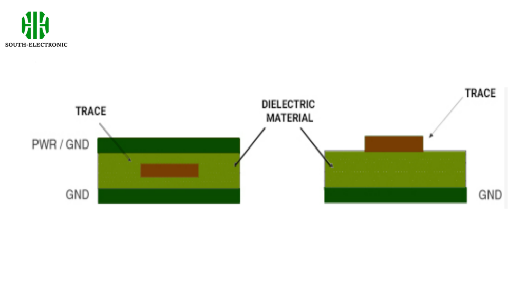
Effectively Manage Impedance in High-Speed PCB Designs
- Controlled Impedance Traces: Use controlled impedance traces to match the characteristic impedance of the signals.
- Impedance Matching: Match the impedance of traces with the connectors and components to minimize signal reflection.
- Use of Differential Pairs: For high-speed signals, use differential pairs to maintain signal integrity and reduce EMI.
- Proper Trace Width and Spacing: Calculate and maintain proper trace width and spacing based on the dielectric material and signal frequency.
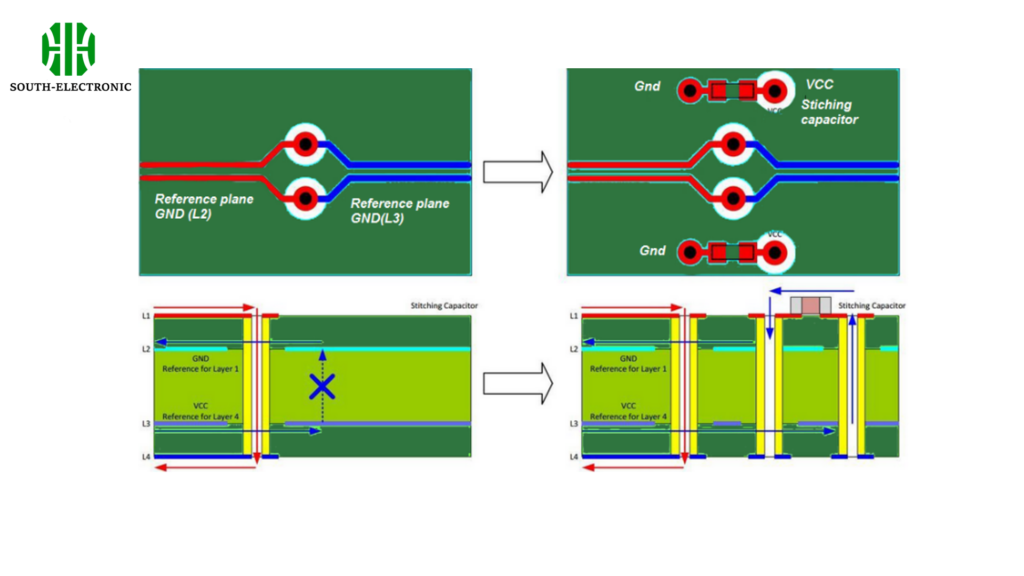
Optimize the Placement of Via
- Minimize Via Usage: Use vias sparingly to reduce signal degradation and maintain signal integrity.
- Use Via-in-Pad for High-Density Designs: For high-density designs, consider using via-in-pad to save space and improve routing.
- Stagger Vias: Avoid placing vias too close to each other to prevent weakening the board structure.
- Thermal Vias for Heat Dissipation: Place thermal vias around heat-generating components to enhance heat dissipation through multiple layers.
Optimizing Power Distribution Networks (PDNs)
- Use Power Planes: Implement dedicated power planes to provide stable voltage and reduce noise.
- Decoupling Capacitors: Place decoupling capacitors close to power pins of ICs to filter out noise and stabilize voltage levels.
- Wide Power Traces: Use wide traces for power distribution to minimize voltage drops and improve current-carrying capacity.
- Proper Via Placement: Ensure adequate vias are used to connect power planes and distribute power evenly across the PCB.


