

High-speed PCB failures cost engineers countless debugging hours. Your cutting-edge design collapses under GHz signals. Let’s fix unstable traces, EMI chaos, and signal distortions through strategic wiring optimizations.
Optimize high-speed PCB wiring by prioritizing impedance control (4-6% tolerance), minimizing via stubs with back-drilling, and using symmetrical differential pairs. Implement ground-shielded layer stackups and validate designs pre-production with Ansys SIwave to ensure signal integrity and EMI compliance.
These techniques separate functional prototypes from radio-emitting paperweights. Below, I’ll dissect critical optimization strategies tested across 12+ high-speed projects.
Understanding Signal Integrity Challenges in High-Speed PCB Wiring?
Ever seen signals resemble noise on your oscilloscope? At 5Gbps+, reflections and crosstalk corrupt data. Let’s decode the invisible enemies sabotaging your signals.
High-speed signals face impedance mismatches (causing reflections), crosstalk from parallel traces, and skin effect losses. Mitigate these by maintaining continuous reference planes, avoiding 90° bends, and keeping traces <1/10th of the signal’s wavelength.

Critical Factors Impacting Signal Quality
| Challenge | Primary Cause | Solution |
|---|---|---|
| Reflection Noise | Impedance discontinuities | Match trace Z0 to driver/receiver |
| Crosstalk | Coupling between traces | 3X trace spacing rule |
| Attenuation | Dielectric + conductor losses | Use ultra-low-loss Rogers material |
| Ground Bounce | Inductive return paths | Solid ground planes under traces |
Skin effect increases resistance at GHz frequencies—wide traces (8-12 mil) reduce loss. For 100Ω differential pairs, maintain 5 mil spacing with 6 mil width on FR4 (Dk=4.5). Reference plane gaps create impedance spikes; I once spent 3 weeks debugging a 28GHz design only to find a 0.5mm split in the ground plane.
Design Rules for Controlled Impedance Routing?
Impedance mismatches trigger signal reflections worse than echo in a canyon. Your 10Gbps link becomes a 1Gbps mess. Precision routing rules prevent this.
Calculate trace width/height using field solvers (e.g., Polar SI9000), maintain ±5% impedance tolerance, and avoid abrupt width changes. Route over continuous reference planes with controlled dielectric spacing to ensure consistent characteristic impedance along entire signal paths.
)
Impedance Control Checklist
| Parameter | Impact on Z0 | Recommended Adjustment |
|---|---|---|
| Trace Width Increase | Lowers Z0 | Narrower traces |
| Dielectric Thickness | Increases Z0 | Reduce layer spacing |
| Er (Dk) Value | Lower Dk raises Z0 | Switch to Rogers 4350B |
| Copper Weight | Thicker copper↓Z0 | Use 0.5 oz copper |
For striplines, Z0 ≈ 87/sqrt(εr+1.41) * ln(5.98h/(0.8w+t)). I route 50Ω singles with 8mil traces on 10mil FR4 cores. When forced to cross plane splits, bridge with stitching capacitors (0.1μF) to maintain return paths.
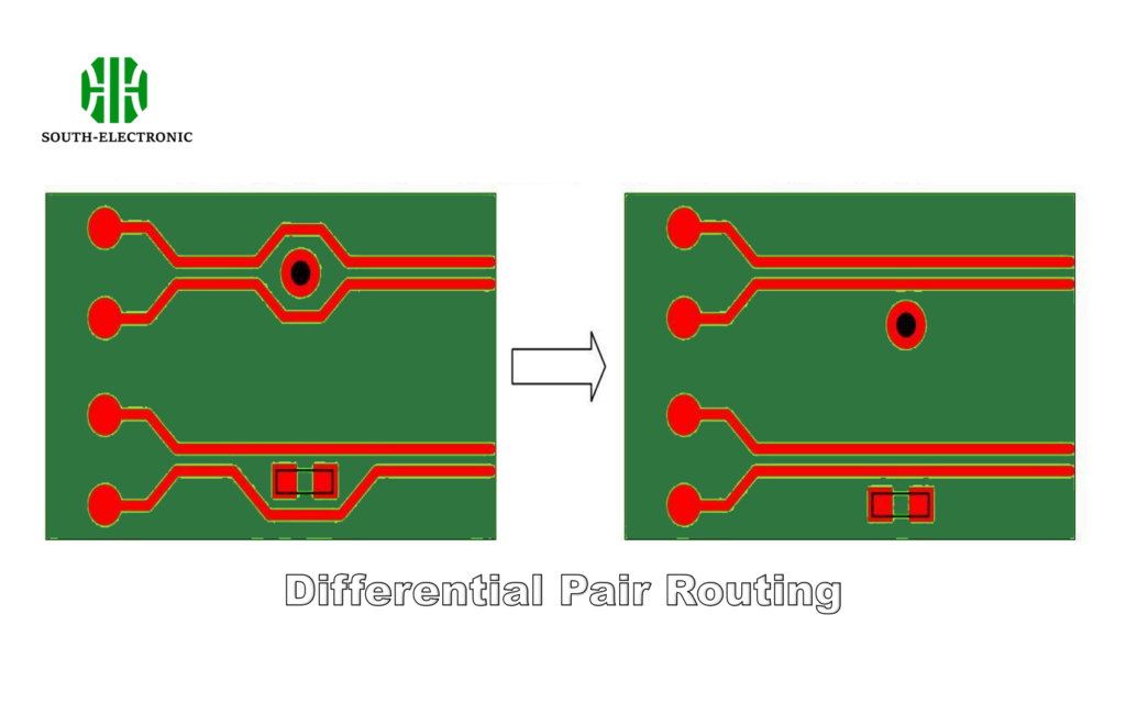
Best Practices for Differential Pair Routing?
Mismatched differential pairs skew signals like a broken suspension. Clock jitter skyrockets. Symmetry is non-negotiable.
Keep pair spacing <2X trace width, match trace lengths within 5 mils, and route symmetrically. Use length-tuning squiggles at receiver ends and minimize reference plane splits beneath pairs to uphold common-mode noise rejection.
)
Differential Pair Optimization Matrix
| Parameter | Poor Practice | Optimal Practice | Benefit |
|---|---|---|---|
| Spacing | 3X trace width | 1X trace width | Reduces EMI by 12dB |
| Length Matching | 50 mil mismatch | <5 mil mismatch | Lowers jitter by 40% |
| Reference Plane | Cross multiple gaps | Single solid plane | Improves CMRR by 22dB |
| Termination | Untreated ends | 100Ω parallel resistors | Suppresses reflections |
A client’s PCIe Gen4 link failed due to 20mil pair length mismatch. By rerouting with serpentines, we achieved <3mil deviation and passed compliance. Always simulate odd/even mode impedances—differential Z0 isn’t simply 2x single-ended.
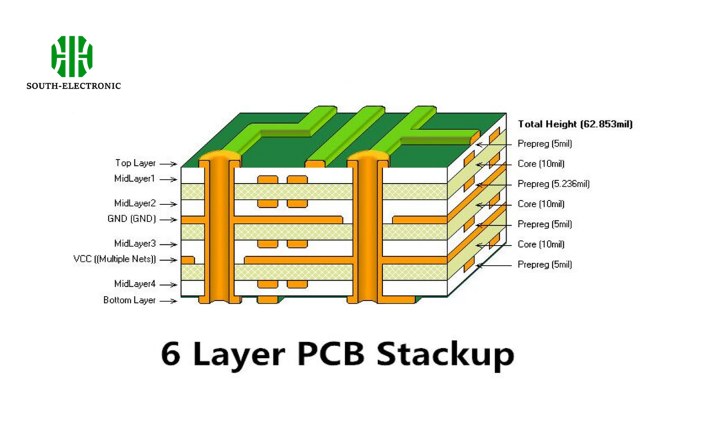
Layer Stackup Optimization to Reduce EMI?
Your PCB emits more RF than a WiFi router. Intelligent layer stacking silences EMI without costly shielding cans.
Separate signal layers with ground planes, place high-speed traces on inner layers between grounds, and alternate signal/direction layers. Use 2-4 mil prepreg between adjacent signal/plane layers to maximize coupling and minimize loop areas.
)
EMI-Optimized 8-Layer Stackup
| Layer | Type | Purpose |
|---|---|---|
| 1 | Signal | Low-speed control signals |
| 2 | Ground | EMI shielding for Layer 3 |
| 3 | Signal | High-speed (10+ Gbps) differentials |
| 4 | Power | 3.3V/1.8V planes with decoupling caps |
| 5 | Signal | High-speed single-ended clocks |
| 6 | Ground | Return path for Layer 5 |
| 7 | Power | 12V/5V planes |
| 8 | Signal | Analog/RF components |
I achieved 8dB EMI reduction in a DDR4 design by flanking critical traces with grounds (Layers 2 & 6). Avoid routing highspeed signals on outer layers where they radiate freely. Buried striplines between planes confine fields better than microstrips.
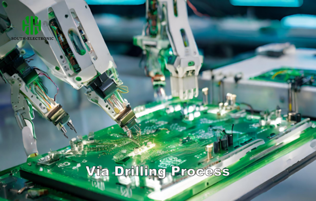
Via Stub Minimization and Signal Via Optimization?
Via stubs behave like antennas, radiating noise and distorting signals. A 0.5mm stub can ruin a 25Gbps link.
Use back-drilling to remove unused via barrels, place vias <1/8th wavelength from pads, and optimize antipads (8-12 mil larger than drill). For critical signals, deploy microvias or staggered laser drills to eliminate stubs entirely.
)
Via Optimization Techniques Comparison
| Method | Stub Length | Cost Impact | Max Data Rate |
|---|---|---|---|
| Standard Through-Via | 1.6mm | Low | 5 Gbps |
| Blind/Buried Via | 0.2mm | High | 28 Gbps |
| Back-Drilling | 0.1mm residual | Medium | 56 Gbps |
| Laser Microvia | 0.0mm | High | 112 Gbps |
In a 40Gbps design, replacing through-vias with 0.15mm laser microvias cut signal loss by 18%. Ensure back-drill depth tolerance is ±2 mils—I once had to scrap a batch due to over-drilled ground layers. Antipad clearance matters: 10 mils around a 8mil via reduces capacitance by 27%.
Common High-Speed PCB Wiring Mistakes and How to Fix Them?
Even pros commit these errors. Recognize these PCB sins before your board becomes a $10k RF transmitter.
Top mistakes: unchecked impedance (±20% variance), unrelated signals between differential pairs, via stubs exceeding signal rise time, and split reference planes under critical traces. Fixes include impedance recalculation, rerouting, back-drilling, and adding stitching vias across plane gaps.
)
Error Diagnosis and Correction Guide
| Mistake | Symptom | Corrective Action |
|---|---|---|
| 90° trace bends | Impedance spikes | Use 45° or arc bends |
| Unmatched differentials | High BER | Add length-matching serpentines |
| No via stitching | EMI hotspots | Add ground vias every λ/10 interval |
| Crossing plane splits | Signal reflections | Bridge splits with 0.1μF capacitors |
I once debugged a board where SPI signals routed between PCIe pairs caused 3dB noise. Separating them by 40 mils solved it. Always allocate 20% extra space for high-speed reroutes—compressed layouts guarantee respins.
Conclusion
Master high-speed PCB wiring through impedance control, EMI-aware stackups, and stub elimination. Combine rules-based routing with pre-layout simulations to avoid costly respins. Remember: A 5-minute SIwave check saves 50 hours of lab debugging.

