

Watching your PCB design fail during prototyping feels like watching money burn. Time constraints, hidden flaws, and costly revisions can derail even well-planned projects. Let’s explore how to navigate these challenges effectively.
Successful PCB proofing[^1] requires balancing design verification with cost control. Focus on component accuracy, perform comprehensive electrical testing, and strategically plan sample quantities. Partnering with reliable suppliers helps catch process errors early to ensure mass production quality.
While these fundamentals set the stage, the real mastery lies in executing four critical strategies. Let’s break down each key aspect to transform your prototyping process from risky to reliable.
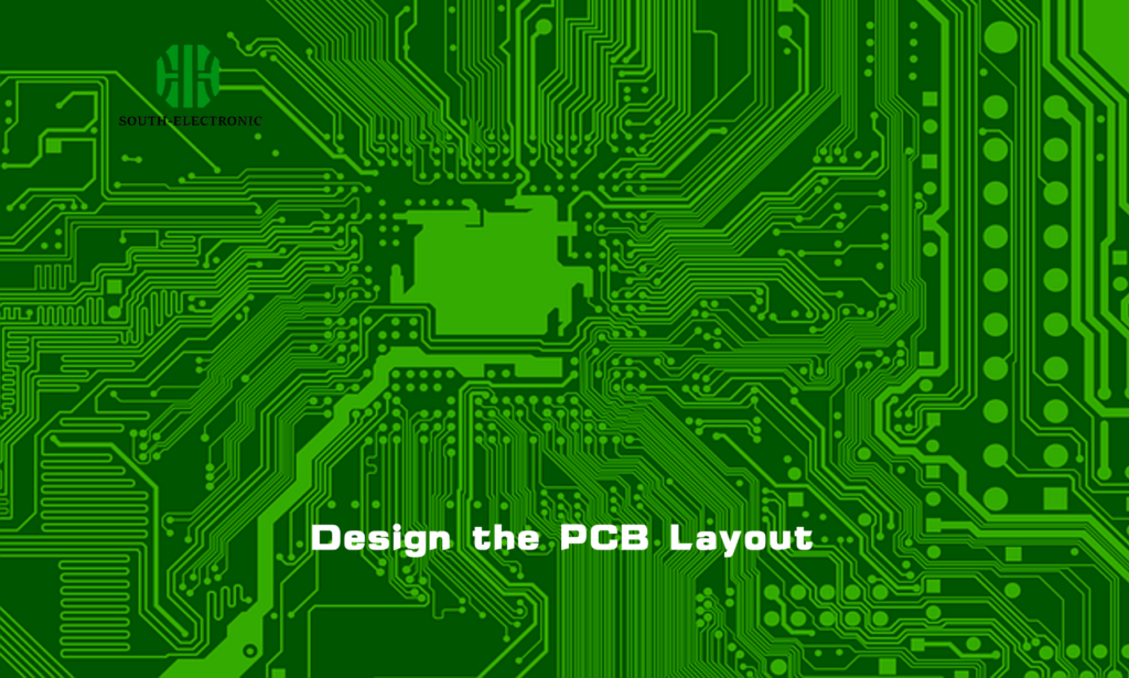
What Precautions Should Be Taken During the PCB Proofing Process?
Imagine discovering a footprint error after manufacturing 100 boards. One overlooked detail can cost weeks of rework. Prevention starts with systematic verification at every stage.
Mandate 3-layer verification: 1) Match component footprints with actual parts 2) Confirm test point accessibility 3) Validate thermal management through simulation. Implement automated optical inspection (AOI)[^2] and boundary scan testing to catch 97% of assembly defects early.
Three Pillars of Effective Proofing
| Verification Stage | Key Activities | Common Pitfalls |
|---|---|---|
| Design Validation | Footprint matching, DFM checks | Incorrect pad sizes |
| Process Selection | Layer stack-up approval, surface finish selection | Impedance miscalculations |
| Testing Protocol | Flying probe + functional testing combo | Incomplete test coverage |
Request your supplier to provide:
- IPC-6012 Class 2 inspection report
- Raw material certifications
- Cross-sectional analysis of plated holes
Conduct thermal cycle testing[^3] beyond standard requirements – I once prevented field failures by testing boards at -40°C to 125°C despite the product’s rated 0-70°C range.
How to Reasonably Control the Number of PCB Proofing to Balance Costs and Testing Requirements?
Ordering 50 prototypes when 10 suffice wastes $1,200+ in most cases. But undersampling risks missing critical flaws. The solution lies in strategic quantity planning[^4].
Calculate sample size[^5] using: (Critical Parameters) × (Test Rounds) + 20% buffer. For boards with 5 high-risk areas needing 3 test iterations, make 5×3×1.2=18 units. Combine multiple tests per board to maximize data per sample.
Smart Quantity Calculation Framework
| Board Complexity Level | Baseline Samples | Additional per High-Risk Feature |
|---|---|---|
| Basic (1-2 layer) | 5 | +2 |
| Moderate (4-6 layer) | 8 | +3 |
| Advanced (HDI/rigid-flex) | 12 | +5 |
Example implementation:
- 6-layer board with DDR4 routing and thermal vias
- Baseline: 8 + 3 (DDR4) + 3 (thermal) = 14 samples
Use staggered prototyping[^6]:
- First batch: 5 units for basic functionality
- Second batch: 10 units for environmental stress
- Final batch: 3 units for compliance testing
How to Choose the Right PCB Design Conversion Software to Improve Board Copying Efficiency?
Converting legacy designs often consumes 40% of reverse engineering time. Tool selection directly impacts how quickly you can modernize existing boards without errors.
Prioritize software with intelligent component recognition (OCR + ML)[^7] and layer alignment automation. Top tools reduce schematic redrawing time by 70% through automatic netlist generation from scanned PCB images.
)
Software Selection Matrix
| Feature | Entry-Level | Professional | Enterprise |
|---|---|---|---|
| Image-to-Schematic | 70% accuracy | 90%+ accuracy | Multi-board support |
| Library Management | Basic | Cloud sync | Legacy part wizard |
| DFM Integration | None | Real-time checks | Full process link |
Proven workflow:
- Scan board → 2. Software aligns layers → 3. Auto-generates component list → 4. Cross-verify critical components
I achieved 60% faster conversions using software that automatically matched obscure SMD codes to modern equivalents. Always cross-check power components manually – automated systems often miss current rating nuances.
What Are the PCB Board Copying Techniques?
Modern board copying goes beyond basic tracing. Missing the shift to smart duplication techniques leaves you vulnerable to counterfeit parts and signal integrity issues.
Implement 3D X-ray tomography[^8] for hidden layer analysis and signal reconstruction algorithms[^9] for damaged boards. Combine these with EMS supplier databases to authenticate components – 23% of copied boards contain mismatched parts.
)
Advanced Copying Methodology
| Technique | Application | Accuracy Boost |
|---|---|---|
| Laser ablation scanning[^10] | Multilayer boards | 99% layer repro |
| IBIS modeling | Signal recreation | 85% waveform |
| Batch component tracing[^11] | BOM verification | 100% matches |
When copying a 12-layer server board:
- Used CT scanning to map blind vias
- Cross-referenced decrypted FPGA code with Intel’s database
- Recreated DDR4 timing through protocol analysis[^12]
Always add 3 modifications to copied designs:
- Improve thermal relief patterns
- Update obsolete component footprints
- Add modern test points
Conclusion
Strategic PCB proofing combines rigorous verification, smart sampling, advanced tools, and supplier collaboration. Focus on extracting maximum data per prototype while maintaining strict cost discipline – this balance defines successful hardware development today.
[^1]: Exploring best practices for PCB proofing can help you avoid costly mistakes and ensure a smoother prototyping process.
[^2]: Understanding AOI’s role in PCB manufacturing can enhance your quality control and reduce assembly defects significantly.
[^3]: Learning about thermal cycle testing can help you ensure your PCB designs withstand extreme conditions, preventing future failures.
[^4]: Understanding strategic quantity planning can help you optimize your PCB prototyping process and reduce costs effectively.
[^5]: Learning how to calculate sample size ensures you have enough prototypes to identify flaws without overspending.
[^6]: Exploring staggered prototyping can enhance your testing strategy, ensuring thorough evaluation at each stage of development.
[^7]: Explore this link to understand how intelligent component recognition can enhance your PCB design process and efficiency.
[^8]: Learn about 3D X-ray tomography and its benefits for hidden layer analysis in PCB design, ensuring better accuracy and reliability.
[^9]: Discover how signal reconstruction algorithms can help in repairing damaged PCBs and improving signal integrity.
[^10]: Explore this link to understand how laser ablation scanning enhances accuracy in multilayer board copying, crucial for modern PCB design.
[^11]: Discover the benefits of batch component tracing for ensuring 100% matches in BOM verification, vital for efficient production.
[^12]: Learn about protocol analysis and its role in accurately recreating DDR4 timing, essential for high-performance server boards.

