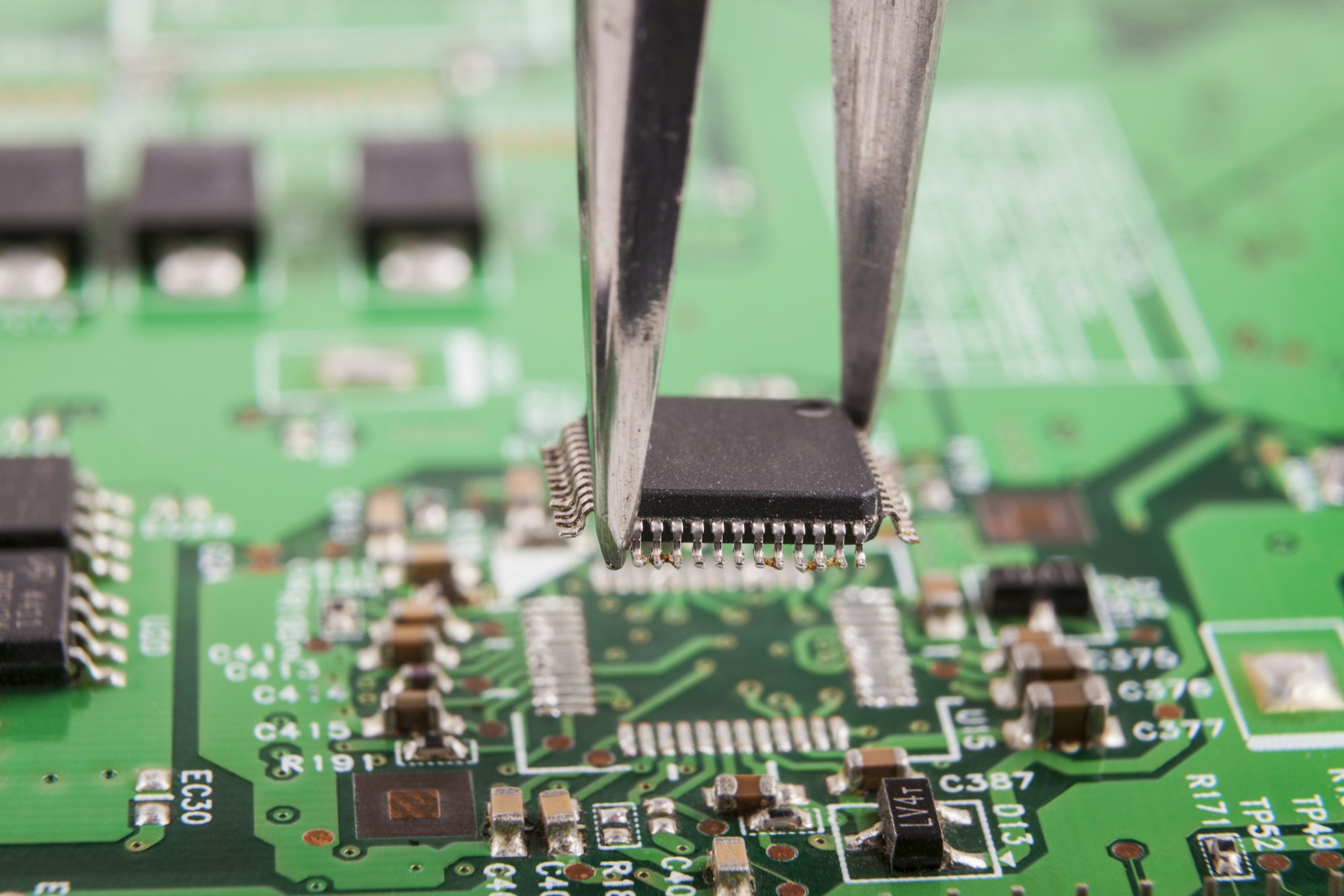
Your PCB design works in simulations, but will it survive real-world manufacturing? One misplaced via or 5-mil spacing error could turn your prototype into scrap metal.
DFM (Design for Manufacturing)[^1] bridges prototyping and mass production. By aligning designs with factory capabilities, DFM eliminates 83%* of respins caused by manufacturing oversights like improper spacing or material incompatibilities.
)
While DFM appears technical, its principles directly impact profitability. Let’s dissect critical failure points that sabotage even "perfect" designs.
5 Critical DFM Mistakes That Derail PCB Production
Picture your board failing due to a $0.02 component placement error. These silent DFM killers waste weeks in redesigns and delay product launches.
Top 5 DFM errors include insufficient edge clearance (shorting), non-standard vias (drill breakage), missing solder dams (bridging), unbalanced copper (warping), and improper panelization (V-cut failures). All preventable through upfront DFM validation[^2].
)
Critical DFM Checklist
| Error Type | Failure Mode | Prevention |
|---|---|---|
| Tight trace spacing | Short circuits | Apply IPC-2221 Class 2 guidelines |
| Non-plated vias | Open connections | Use 0.2mm min hole with 0.1mm ring |
| Missing thermal pad | Cold solder joints | Implement 4-spoke thermal relief |
| Unbalanced copper | Board warping | Maintain ±10% layer distribution |
| Poor panelization | Broken breakaway tabs | Use 3mm edge clearance with mousebites |
During automated assembly, even 0.1mm via placement errors can fracture components. In one project, redesigning 6-layer boards three times cost us $15k after discovering the CM’s drill couldn’t handle 0.15mm microvias.
5 Critical DFM Mistakes That Derail PCB Production
Picture your board failing due to a $0.02 component placement error. These silent DFM killers waste weeks in redesigns and delay product launches.
Top 5 DFM errors include insufficient edge clearance (shorting), non-standard vias (drill breakage), missing solder dams (bridging), unbalanced copper (warping), and improper panelization (V-cut failures). All preventable through upfront DFM validation.
)
Critical DFM Checklist
| Error Type | Failure Mode | Prevention |
|---|---|---|
| Tight trace spacing | Short circuits | Apply IPC-2221 Class 2 guidelines |
| Non-plated vias | Open connections | Use 0.2mm min hole with 0.1mm ring |
| Missing thermal pad | Cold solder joints | Implement 4-spoke thermal relief |
| Unbalanced copper | Board warping | Maintain ±10% layer distribution |
| Poor panelization | Broken breakaway tabs | Use 3mm edge clearance with mousebites |
During automated assembly, even 0.1mm via placement errors can fracture components. In one project, redesigning 6-layer boards three times cost us $15k after discovering the CM’s drill couldn’t handle 0.15mm microvias.
Layer Stackup Secrets
Your layer stackup[^3] dictates both electrical performance and manufacturability. Wrong material choices can inflate costs 40% or create impedance nightmares.
Optimal stackups balance electrical needs with factory capabilities. Consider core thickness tolerance (±10%), dielectric Dk consistency, and copper type[^4] (e.g., HVLP vs. RA).
)
Stackup Design Matrix
| Parameter | Standard Board | High-Speed | Flex-Rigid |
|---|---|---|---|
| Core thickness | 1.6mm±10% | 0.8mm±5% | 0.2mm coverlay±0.02mm |
| Copper weight | 1oz | 0.5oz outer/1oz inner | Rolled copper 12μm |
| Dielectric material | FR-4 Tg130 | Rogers 4350B | Polymide |
| Impedance control | ±20% | ±10% | ±8% with laser drill |
Switching from standard FR-4 to Isola 370HR last quarter reduced warping 22% post-lamination, saving three days in machine calibration. Always verify material specs against factory stock.
Conclusion
DFM transforms designs into manufacturable products. Verify factory capabilities early to prevent 90% of delays and eliminate hidden cost sinks.
[^1]: Understanding DFM is crucial for ensuring your PCB designs are manufacturable, reducing costs and time delays.
[^2]: Exploring DFM validation techniques can significantly enhance your design’s manufacturability and reliability.
[^3]: Exploring layer stackup insights can enhance your PCB design, optimizing both performance and manufacturability.
[^4]: Learning about various copper types can help you make informed decisions for your PCB projects, improving reliability and performance.


