
Ever mixed up PCB and PCBA while ordering parts? This confusion costs time and money. Let’s cut through the jargon to clarify these terms for your next project.
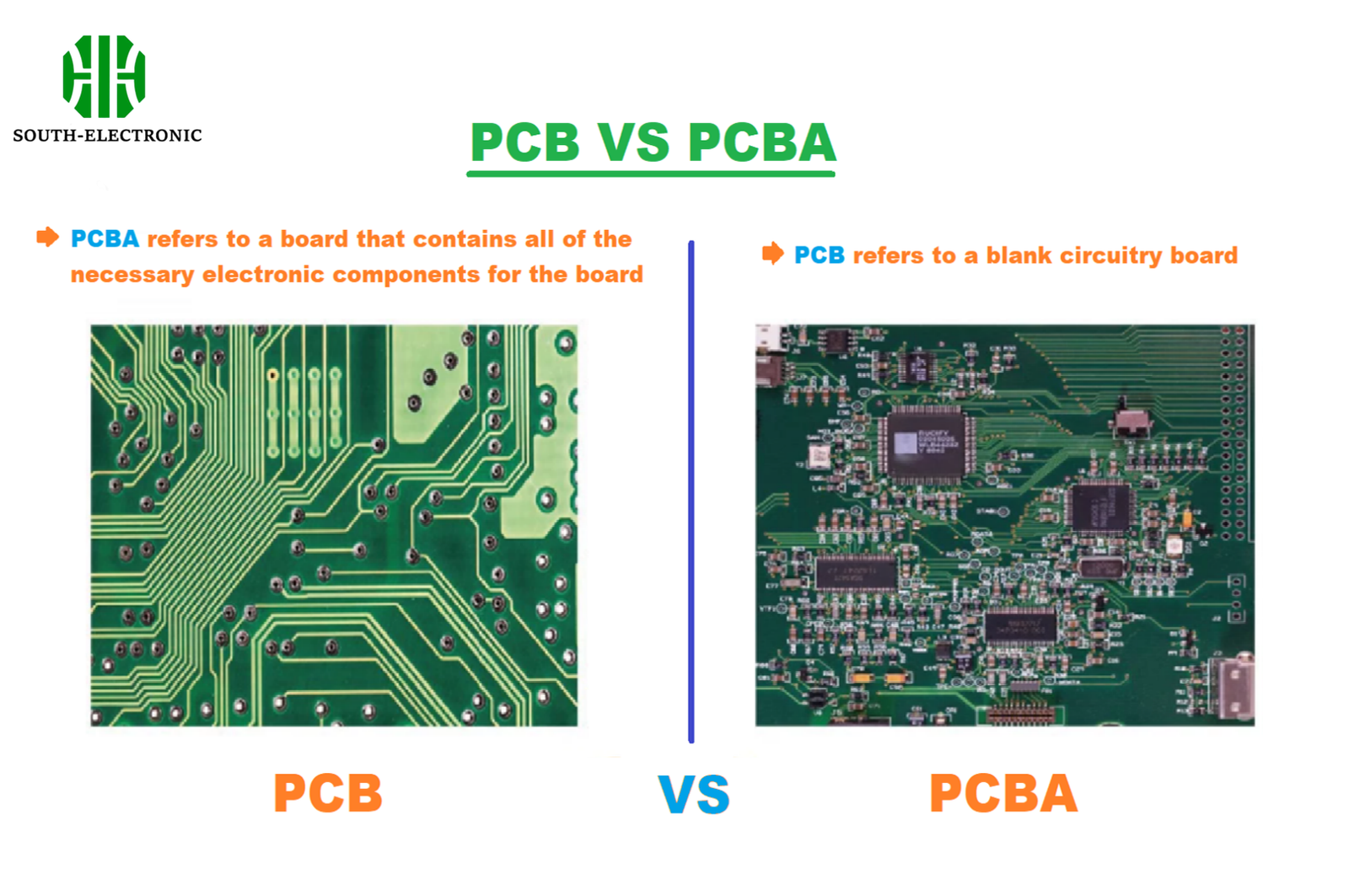
PCB is the "blank canvas" – a bare circuit board without components. PCBA is the "finished painting" – a fully assembled board with soldered parts[^1] that make it functional.
Understanding this distinction impacts your design workflow and budgeting. Let’s dive deeper into their definitions, production steps, testing, and cost factors.
What Exactly Do PCB and PCBA Stand For?
Using the wrong term can derange your supplier discussions. Let’s decode these acronyms once and for all.
PCB means Printed Circuit Board – a laminated board with copper traces. PCBA stands for Printed Circuit Board Assembly[^2], referring to a PCB populated with components like resistors and ICs.
)
Core Definitions and Applications
| Aspect | PCB | PCBA |
|---|---|---|
| State | Bare board | Functional assembly |
| Components | None | Soldered parts (SMD/through-hole) |
| Functionality | Non-operational | Ready for end-use |
| Usage | Prototyping, custom builds | Electronics in devices |
Think of PCB as raw dough and PCBA as baked pizza. PCBs provide pathways for signals, while PCBA brings those pathways to life with components. For IoT startups, ordering PCBAs upfront prevents assembly delays in product launches.
How Does the Manufacturing Process Differ Between PCB and PCBA?
Mixing up PCB and PCBA steps wastes resources. Let’s break down their production journeys.
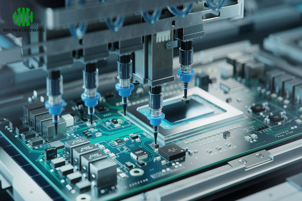
PCB manufacturing[^3] involves etching copper layers. PCBA adds precise component placement using pick-and-place machines followed by reflow soldering.
)
Step-by-Stage Comparison
| Stage | PCB | PCBA |
|---|---|---|
| Design | Layout creation | Bill of Materials (BOM) prep |
| Fabrication | Copper etching, drilling | Solder paste application |
| Assembly | Not applicable | Component mounting |
| Quality Check | Continuity testing | Functional testing |
A client once ordered 100 PCBs thinking they’d arrive ready-to-use. They later realized they needed PCBA services for soldering components, delaying their product launch by three weeks. Always verify requirements with your manufacturer!
How Are Testing Methods Different for PCB and PCBA?
Skipping appropriate tests risks dead boards. Learn which checks apply to each stage.
PCB testing[^4] focuses on electrical connectivity. PCBA testing validates component functionality – like checking if a sensor sends data correctly.
)
Testing Protocols
| Test Type | PCB Checks | PCBA Checks |
|---|---|---|
| Electrical | Shorts/open circuits | Power-on functionality |
| Visual | Trace alignment | Solder joint quality |
| Functional | N/A | Firmware/component interaction |
A robotics team I worked with found 20% of their PCBs had microscopic cracks. Post-PCBA, faulty boards would’ve cost 5x more to rework. Early PCB testing saved $12k in potential losses.
Why Is PCB Assembly So Expensive?
PCBA quotes often shock newcomers. Let’s dissect what drives these costs.
Component sourcing, labor, and precision equipment raise PCBA costs. Automation reduces pricing but has upfront setup fees.
Cost Contributors
| Factor | PCB Cost Impact | PCBA Cost Impact |
|---|---|---|
| Materials | Copper, laminate | ICs, connectors, solder |
| Labor | Lower (automated etching) | Higher (manual inspection) |
| Machinery | Laser drills | Pick-and-place systems |
| Minimum Orders | Often lower | Higher due to component MOQs |
A wearable startup opted for cheaper connectors during PCBA. Later, 30% failed during drop tests, costing more than using pricier-rated parts. Never compromise on component quality[^5] for critical applications.
Conclusion
PCB is the unpopulated board; PCBA is its functional version with components. From design to testing, each stage demands precise workflows to avoid costly reworks. Choose your manufacturing partner wisely!
[^1]: Learn about soldered parts and their significance in creating functional electronic assemblies. This knowledge is vital for your projects!
[^2]: Understanding PCBA is crucial for ensuring your electronic devices function correctly and efficiently. Explore this link to learn more.
[^3]: Discover the intricate process of PCB manufacturing to enhance your knowledge and improve your project outcomes. Click to learn more!
[^4]: Understanding PCB testing best practices can help ensure quality and reliability in your electronic designs.
[^5]: Learning about the impact of component quality on PCBA performance can guide better sourcing decisions for your projects.

