
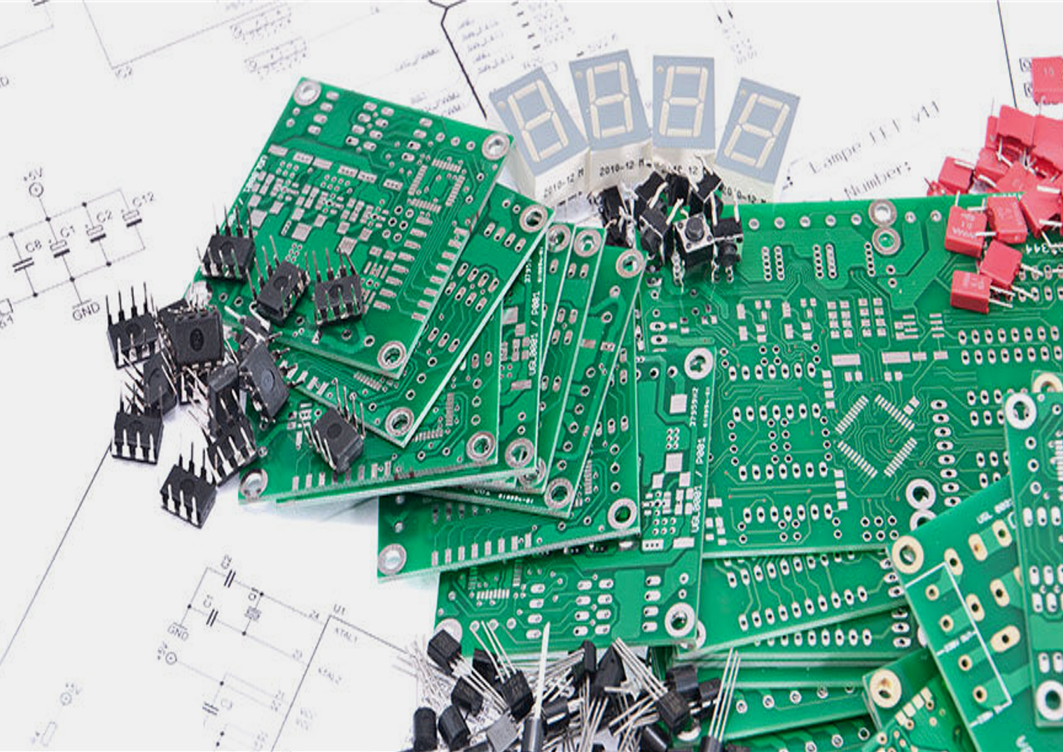
What is PCB Assembly?
PCB assembly is the process of soldering electronic components onto a printed circuit board (PCB) to create a working electronic device. This process involves several steps, including applying solder paste, placing components, soldering, and inspecting.
Steps of PCB Assembly
Understanding the PCB assembly process is key. It helps you design better, troubleshoot better, and innovate better in your projects. It also helps you choose the right assembly techniques and tools, so that your final product meets quality and functionality standards.
1. Solder Paste Application
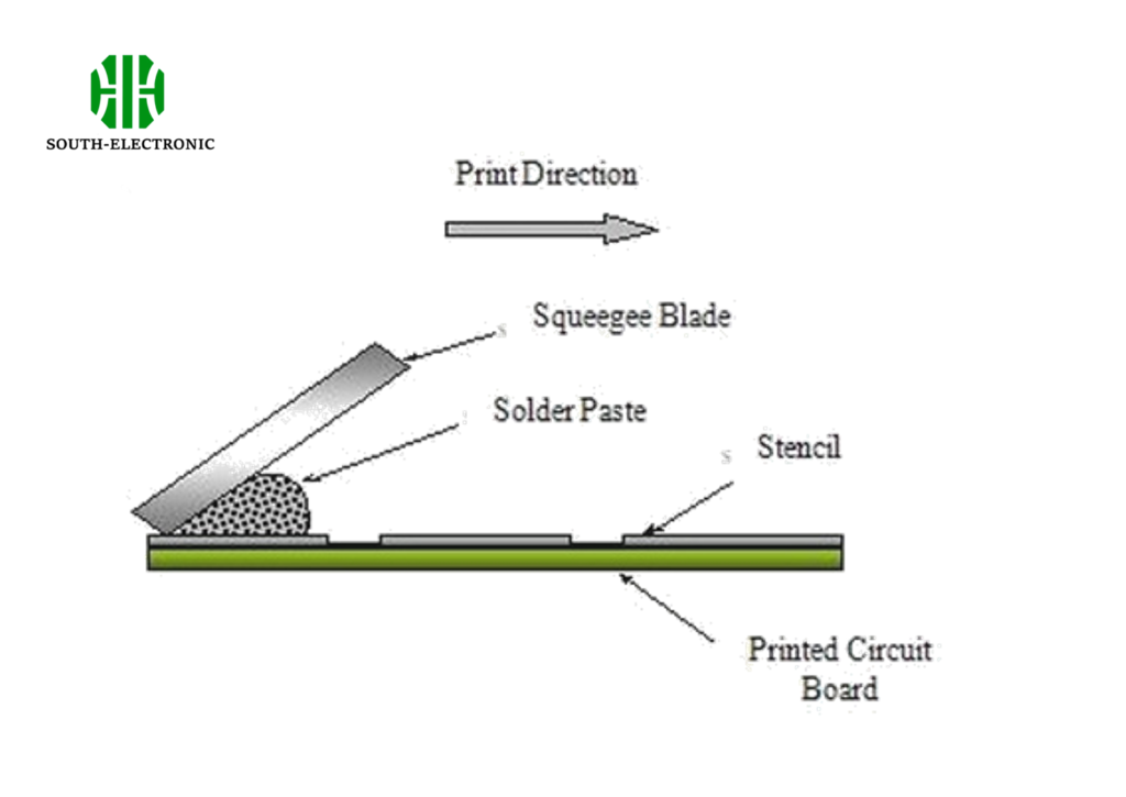
The first step in PCB assembly is the application of solder paste to the PCB. This paste is a mixture of tiny solder particles and flux, which helps in bonding the electronic components to the board. The solder paste is applied using a stencil that matches the PCB’s layout.
Solder Paste Application Process
| Step | Description |
|---|---|
| 1 | Align the stencil with the PCB. |
| 2 | Apply solder paste over the stencil. |
| 3 | Remove the stencil to leave solder paste on the PCB pads. |
| 4 | Inspect for any misalignment or excess paste. |
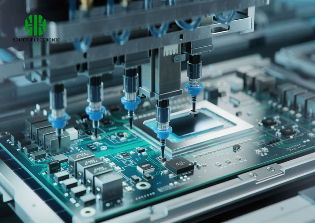
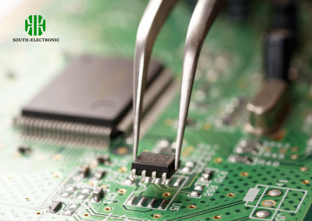
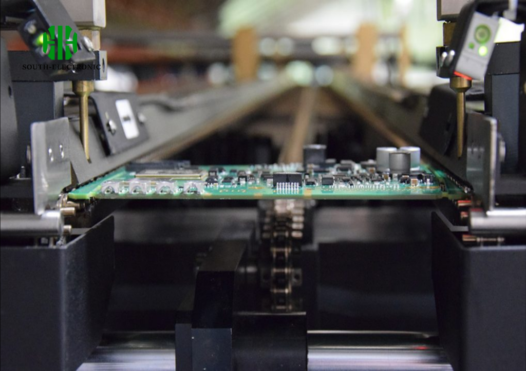
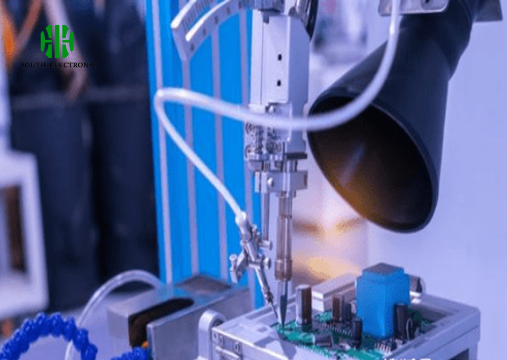
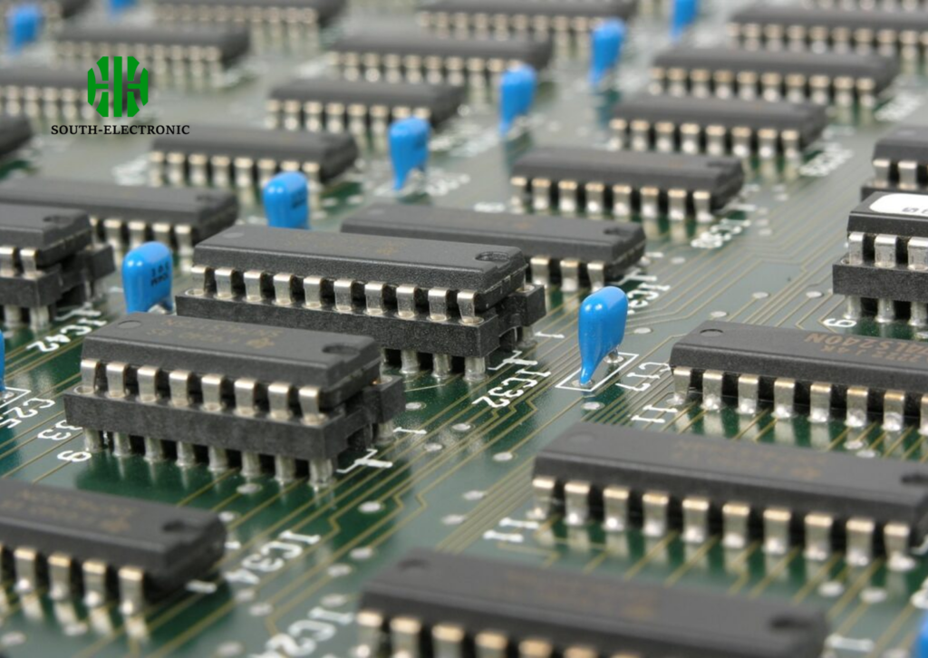
2. Component Placement
The first step in PCB assembly is the application of solder paste to the PCB. This paste is a mixture of tiny solder particles and flux, which helps in bonding the electronic components to the board. The solder paste is applied using a stencil that matches the PCB’s layout.
3. Reflow Soldering
Once the components are in place, the PCB goes through reflow soldering. The board is run through a reflow oven, where the solder paste melts and then cools, creating solid connections between the components and the PCB.
4. Inspection and Quality Control
After reflow, we inspect the PCB for any defects. We use Automated Optical Inspection (AOI) systems to check for things like poor solder joints or misplaced components. Sometimes we even use X-ray inspection, especially for complex boards.
Common Inspection Methods
| Method | Purpose | Example Issue Detected |
|---|---|---|
| AOI | Visual inspection for defects | Misplaced components |
| X-ray | Inspecting solder joints under components | Incomplete soldering |
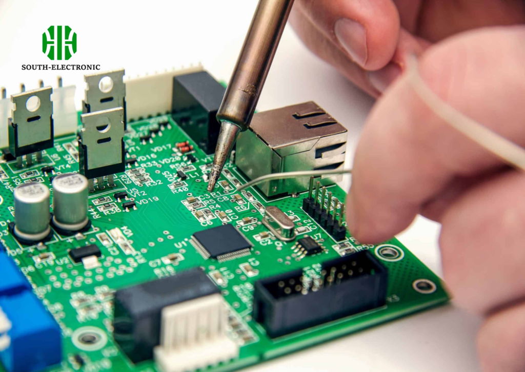
5. Through-Hole Component Insertion
For stuff that needs through-hole soldering, you gotta put the parts in the board. You can do this by hand or with a machine.
6. Final Inspection and Testing
The last thing we do in the PCB assembly process is test the boards. We test them to make sure they work the way they’re supposed to. We also look at them and use electrical tests to make sure there aren’t any problems with them. We want to make sure they’re perfect before we ship them.

How is a PCB Manufactured Step by Step?
Before PCB assembly, the board itself must be manufactured. This process involves several stages:
1. Designing the PCB
The first thing you need to do when making a PCB is design the board. This means creating the schematic and layout using CAD software. Once you have the design finished, you need to review it to make sure it meets all the specifications.
2. Printing the PCB Design
The design is printed on copper-clad laminate using a photolithographic process. This step defines the circuit pattern on the board.
3. Etching and Layer Alignment
The PCB gets etched to remove excess copper, leaving the circuit pattern. Multiple layers are aligned and bonded together to make a multilayer PCB.
4. Solder Mask Application and Silkscreening
Once the circuit is finished, we apply a solder mask to the PCB. The solder mask is a layer of polymer that protects the circuit from the environment and prevents solder bridges. After that, we use a process called silkscreening to print labels and component markings on the board.
Manual vs. Automated PCB Assembly Processes
Manual PCB Assembly
Manual PCB assembly is all about hand-placing components and soldering them onto the PCB. This is perfect for small production runs or when you’re prototyping and need to be flexible and customize things.
Automated PCB Assembly
Automated PCB assembly is awesome because it uses machines to do all the hard stuff like putting the solder paste on the board, placing all the components, and then heating it up to melt the solder. This is the way to go if you’re making a lot of boards because it’s fast, accurate, and it does the same thing every time.
Manual vs. Automated Assembly
| Aspect | Manual Assembly | Automated Assembly |
|---|---|---|
| Speed | Slower | Faster |
| Precision | Variable | High precision |
| Ideal for | Prototyping, small runs | Mass production |
| Setup Cost | Low | High |
| Flexibility | High | Lower compared to manual |
Common Defects in PCB Assembly and How to Avoid Them
- Solder Bridges:Solder bridges happen when you have too much solder and it connects two pins that are next to each other, causing a short. You can avoid this by having a good stencil design and by applying the solder paste accurately.
- Cold Joints:Cold joints happen when the solder doesn’t fully melt, which means you don’t get a good connection. You can avoid this by having the right reflow soldering profiles.
- Misaligned Components:Misalignment happens when you’re doing the pick and place and things aren’t lined up right. You can avoid this by having good maintenance and calibration on your pick and place machines.
- Inspecting for Defects:You can use AOI (automated optical inspection) and X-ray inspection to find problems early in the process, so you can fix them before you build the final product.
If you’re working with electronics, you need to know about the PCB assembly process. It doesn’t matter if you’re designing, manufacturing, or troubleshooting PCBs, understanding this process helps you make high-quality and reliable electronic products. By following the steps in this guide and avoiding common mistakes, you can make sure your PCB assemblies work and last.

