
Imagine your high-speed circuit suddenly distorting video streams or crashing AI computations. Signal reflections from imperfect vias silently sabotage performance. Back drilling surgically removes these invisible enemies. Here’s how this unsung hero cleans up signals in cutting-edge electronics.
PCB back drilling[^1] removes excess copper stubs from through-hole vias using controlled-depth drilling, improving signal integrity[^2] in high-frequency applications[^3] like 5G routers, AI processors, and aerospace-grade multilayer PCBs. This process minimizes signal reflections that degrade data transmission quality.
While the concept sounds straightforward, the technical execution separates mediocre boards from premium ones. Let’s dissect the critical aspects that make back drilling both essential and challenging in modern PCB production.
What Exactly is PCB Back Drilling?
A drone’s GPS module fails mid-flight. An MRI machine produces ghosted images. Both could trace errors to copper stubs in plated through-holes. Back drilling targets these residual conductors like a microscopic excavation tool.
Back drilling removes unused portions of copper barrels in drilled vias using a secondary drilling pass with precise depth control. This eliminates impedance discontinuities that reflect high-frequency signals, working like noise-canceling headphones for your circuit board.
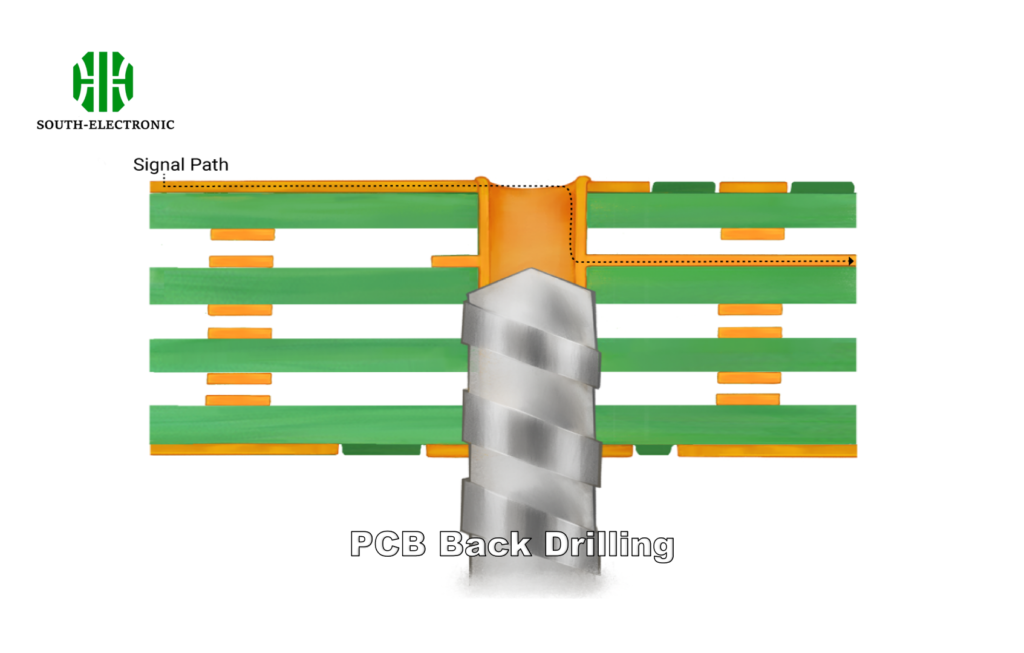)
Copper Stub Elimination Mechanism
Three factors determine back drilling success:
| Parameter | Impact Threshold | Measurement Method |
|---|---|---|
| Stub Length Tolerance | ±75µm | Time-domain reflectometry (TDR) |
| Hole Position Accuracy | ±50µm | Automated optical inspection |
| Drill Bit Wear | >5% diameter loss | Laser micrometrology |
Industrial practice shows stubs exceeding 1/10th wavelength of the signal frequency create measurable distortion. For a 25GHz DDR5 interface, this translates to 1.2mm maximum allowable stub length. Production-grade back drilling achieves under 0.05mm accuracy through servo-controlled spindles and real-time depth monitoring.
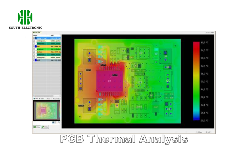
Why Thermal Profiling is the Heart of Successful Reflow?
A telecom company scrapped 20,000 boards when resin smeared during drilling. The culprit? Impropre drilling temperatures altered material behavior. Precise thermal management makes or breaks back drilling[^4] outcomes.
Optimal thermal profiling[^5] maintains PCB material stability during back drilling. It balances heat generation from friction with material Tg points, preventing resin softening that causes hole wall roughness exceeding 10µm RA.
)
Temperature-Zone Strategy
Modern back drilling systems implement three-stage thermal control:
| Stage | Temperature Range | Purpose |
|---|---|---|
| Pre-heat | 85-95°C | Stress relief without Tg approach |
| Active Drilling | 105-120°C | Maintains material consistency |
| Cool-down | 60°C gradient/min | Prevents Z-axis delamination |
FR-4 materials demand tighter control than Rogers substrates. High Tg FR-4 (180°C rating) allows drilling at 140°C for 15% faster feed rates, while PTFE-based boards need cryogenic cooling to -20°C for clean hole walls. Thermal cameras with 0.5°C resolution map heat distribution across drill zones.
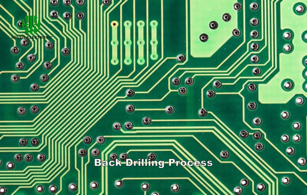
How Does PCB Back Drilling Work?
A server motherboard failed EMI certification due to 12ps signal jitter – solved by modifying back drill overlap parameters. The process marries mechanical precision with material science.
Controlled-depth back drilling[^6] uses modified CNC machines with 0.01mm positioning accuracy. After initial via plating, a slightly larger drill removes excess copper from non-connection layers based on predefined depth maps from CAD files.
)
Process Flow Optimization
Key operational parameters vary by layer count:
| PCB Layers | Typical Speed | Spindle RPM | Retract Rate | Overlap Factor |
|---|---|---|---|---|
| 8-layer | 1.2 m/min | 140,000 | 8 mm/sec | 1.2X hole diam |
| 16-layer | 0.8 m/min | 110,000 | 5 mm/sec | 1.5X hole diam |
| 24-layer | 0.5 m/min | 85,000 | 3 mm/sec | 2.0X hole diam |
The 2023 IPC-6012EM standard mandates 5GHz | 2.0mm | <1.2mm |
| Rising Time | 250ps |
| Production Volume | 100,000 units |
| Bit Error Rate Tolerance| 1e-6 |
Hybrid approaches gain traction – one defense contractor saved $2.1M/year combining partial back drilling (only for >10GHz lines) with via-in-pad techniques[^7] on lower-frequency sections. New conductive fill materials promise 50% stub reduction without drilling for certain applications.
Conclusion
Back drilling transitions PCBs from commodity parts to precision instruments. Mastering its thermal, mechanical and economic variables unlocks reliable high-frequency performance – a critical edge in our 5G and AI-driven world. Always validate through signal integrity testing and cost-benefit analysis.
[^1]: Explore this link to understand how PCB back drilling enhances performance in high-frequency applications, crucial for modern electronics.
[^2]: Learn about the significance of signal integrity in electronics and how it affects data transmission quality in advanced technologies.
[^3]: Discover the challenges faced in high-frequency applications and how innovations like back drilling address these issues effectively.
[^4]: Exploring back drilling techniques can enhance your knowledge of PCB performance and manufacturing efficiency.
[^5]: Understanding thermal profiling is crucial for optimizing PCB manufacturing processes and ensuring material stability during drilling.
[^6]: Explore this link to understand how controlled-depth back drilling enhances PCB performance and reliability, crucial for high-frequency applications.
[^7]: Discover how via-in-pad techniques can improve PCB layout efficiency and performance, especially in high-frequency applications.

