

Step-by-Step PCB Design Guide
1. Understand the Electrical Parameters
Before starting the design, it’s crucial to understand the electrical requirements of your project. This includes knowing the voltage, current, and power ratings of the components and the overall circuit.
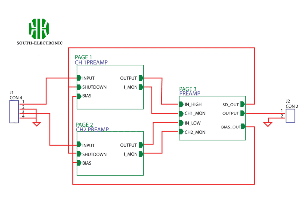
2. Creating the Schematic
Using schematic capture tools, create a detailed circuit diagram. This step involves selecting the appropriate components and defining their connections.
3. PCB Layout
Transfer your schematic to a PCB layout tool. This software helps you design the physical layout of your PCB, placing components and routing connections.
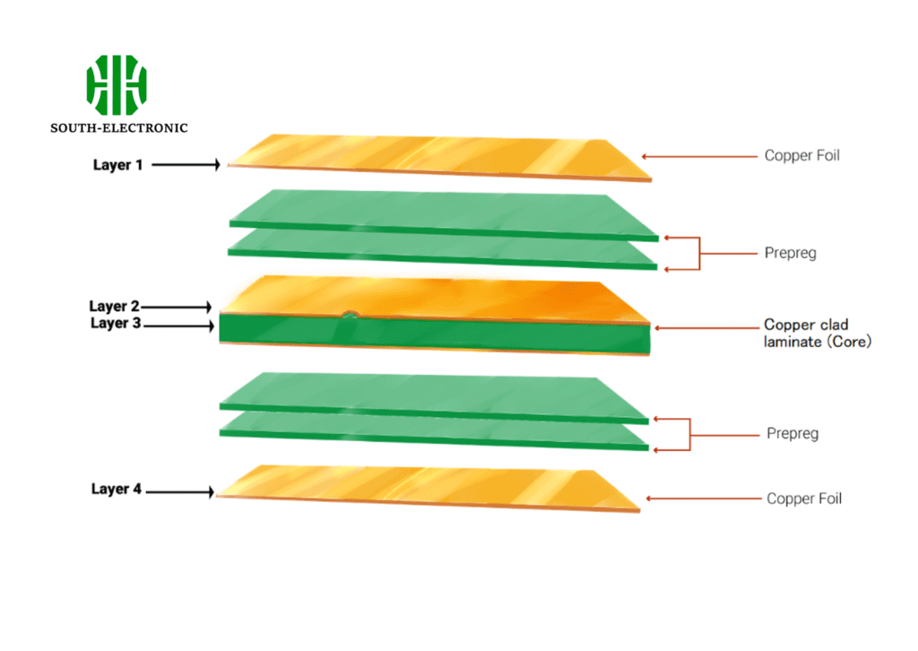
4. Design the Stackup
Plan the layers of your PCB. A simple board might have only one or two layers, while more complex designs can have multiple layers.
5. Define Design Rules
Set design rules and constraints, such as trace width, spacing, and via sizes. These rules ensure your PCB can be manufactured reliably.
6. Component Placement
Place components on the board according to your design. Consider factors like heat dissipation, signal integrity, and accessibility for soldering.
7. Insert Drill Holes
Add holes for component leads and vias. Ensure the holes are accurately positioned and sized for the components.
8. Route the Traces
Connect the components with electrical traces. Keep the traces short and direct to minimize resistance and inductance.
PCB Design Tools Comparison:
| Tool Name | Features | Cost | Best For |
|---|---|---|---|
| KiCad | Open-source, multi-layer support | Free | Beginners, hobbyists |
| EasyEDA | Online tool, simulation capabilities | Free/Paid | Students, hobbyists |
| Autodesk Eagle | Professional-grade, extensive libraries | Paid | Professionals, B2B |
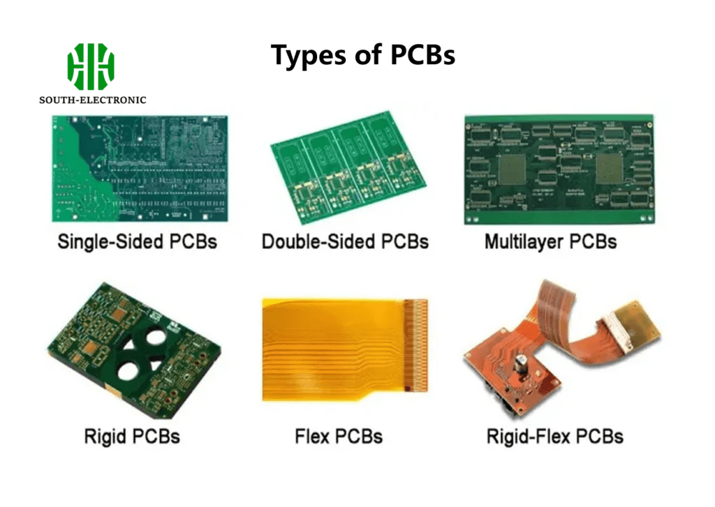
Types of PCBs
Single-Sided:
A single-sided PCB has one layer of conductive material. It’s used in simple, low-cost applications.
Double-Sided:
Double-sided PCBs have conductive material on both sides of the board, allowing for more complex circuits.
Multilayer:
Multilayer PCBs consist of multiple layers of conductive material, separated by insulation. They are used in high-density applications.
Rigid, Flex, and Rigid-Flex:
- Rigid PCBs: Made from a solid substrate, they are durable and stable.
- Flex PCBs: Made from flexible materials, they can bend and twist, suitable for wearable devices.
- Rigid-Flex PCBs: Combine rigid and flexible sections, offering both durability and flexibility.
Common Mistakes to Avoid in PCB Design
- Overcrowding Components: Leave enough space for soldering and heat dissipation.
- Ignoring Thermal Management: Consider heat sinks and ventilation to manage heat.
- Overlooking Manufacturability: Design with manufacturing capabilities in mind to avoid issues during production.
- Skipping Design Reviews: Always review your design with peers or mentors to catch potential errors.
Additional Resources for PCB Design
- Online Forums: Communities like Reddit and Stack Exchange offer valuable advice and troubleshooting tips.
- Tutorials: Websites like SparkFun and Adafruit provide step-by-step guides and tutorials.
- Books: “The Art of PCB Design” and other reference materials can deepen your understanding of PCB design.

