
What is the Main PCB Failure?
The main types of PCB (Printed Circuit Board) failures include:
- Solder Joint Issues: Cracks or poor connections in solder joints can cause intermittent or complete failure of the circuit.
- Component Failures: Defective or improperly installed components can lead to malfunction.
- Delamination: Separation of PCB layers, which can cause electrical discontinuity.
- Trace Damage: Broken or damaged conductive traces interrupt the circuit.
- Thermal Stress: Excessive heat can damage components and solder joints.
- Environmental Factors: Moisture, dust, and contaminants can cause corrosion and shorts.
What are SomeSigns of PCB Failure?
- Visual Damage: Burn marks, discoloration, or visible cracks.
- Intermittent Operation: Devices working sporadically or resetting unexpectedly.
- Complete Failure: Device not powering on or functioning at all.
- Heat Generation: Excessive heat from specific areas of the PCB.
- Unusual Smells: Burning smell indicating potential component or board damage.
- Corrosion: Visible corrosion on solder joints or components.
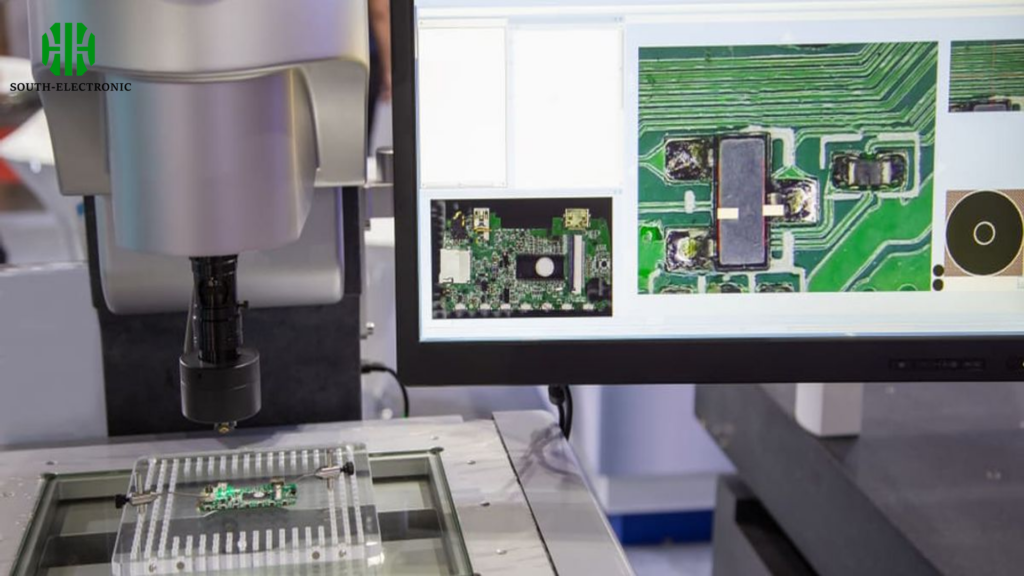
How does Automated Optical Inspection (AOI) Contribute to Identifying PCB Defects?
Automated Optical Inspection (AOI) plays a critical role in identifying PCB defects:
- Visual Inspection: AOI systems use high-resolution cameras to capture images of PCBs and compare them to a pre-defined standard.
- Detection of Solder Issues: Identifies solder joint defects such as insufficient solder, bridging, or solder balls.
- Component Verification: Ensures correct component placement, orientation, and absence of missing components.
- Trace Defects: Detects broken or shorted traces and other surface defects.
- Real-Time Feedback: Provides immediate feedback, allowing for quick correction of errors in the manufacturing process.
Benefits of AOI in PCB Manufacturing:
| Benefit | Description |
|---|---|
| Early Defect Detection | Identifies defects before assembly completion |
| High Accuracy | Uses high-resolution cameras for precise inspection |
| Reduced Costs | Minimizes rework and scrap costs |
| Increased Efficiency | Speeds up the inspection process compared to manual checks |
| Consistent Quality | Ensures uniform quality across all produced PCBs |
How can regular maintenance prevent PCB failures?
Regular maintenance can significantly reduce the risk of PCB failures:
- Inspection: Regularly inspect for signs of wear, damage, and corrosion.
- Cleaning: Keep PCBs clean from dust, dirt, and contaminants using appropriate cleaning methods.
- Thermal Management: Ensure proper cooling and ventilation to prevent overheating.
- Environmental Control: Protect PCBs from moisture and corrosive environments.
- Component Testing: Periodically test components for functionality and replace any that show signs of failure.
- Firmware Updates: Ensure that the firmware is up-to-date to avoid compatibility and performance issues.
PCBs (Printed Circuit Boards) can fail due to various reasons such as exposure to moisture, dust, extreme temperatures, and physical damage. Understanding the signs of PCB failure and employing preventative measures like Automated Optical Inspection (AOI) and regular maintenance can help mitigate these risks and ensure the longevity of your PCBs.

