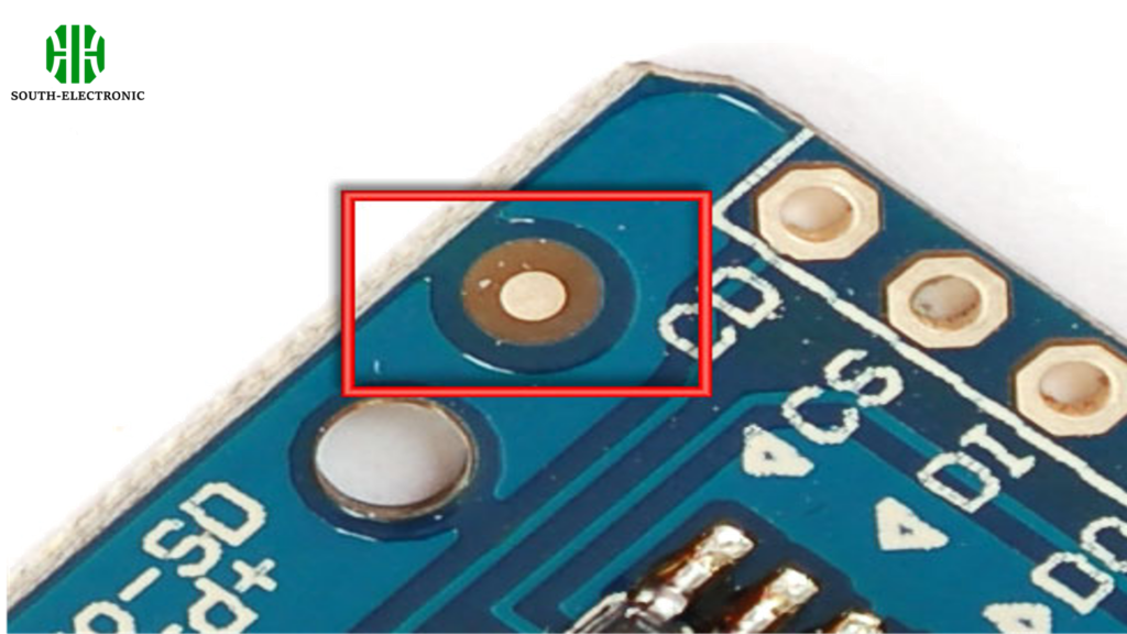
What is PCB Fiducial Mark?
Fiducial marks are specifically placed reference points on a PCB used primarily by automated assembly machines to ensure accurate positioning of components. These marks are essential for minimizing errors in the assembly process, particularly in high-density or highly precise manufacturing environments.
What are the types of PCB Fiducial Marks?
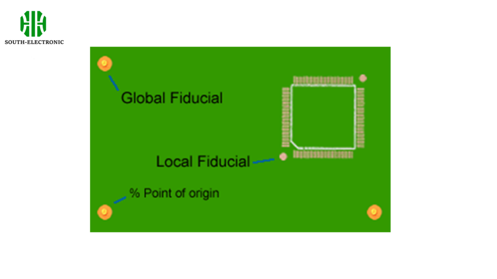
Fiducial marks on PCBs (Printed Circuit Boards) are reference points used to ensure accurate alignment during manufacturing. There are mainly three types:
- Global Fiducials: These marks help position the board itself within the assembly or soldering machine. They are typically placed on the corners of the PCB.
- Local Fiducials: These are used for aligning specific components on the PCB, especially those requiring high precision like BGAs (Ball Grid Arrays). They are located near the components they reference.
- Panel Fiducials: When PCBs are manufactured in panels containing multiple boards, these marks help align the entire panel in the assembly equipment. They are placed on the edges of the panel, outside the individual boards.
What are the standard sizes and shapes for PCB fiducial marks?

| Shape | Size (Diameter) | Common Uses |
| Circular | 1mm | Used in high-precision devices for component alignment |
| Circular | 2mm | Standard size for general PCB manufacturing |
| Square | 1mm x 1mm | Used where more distinct geometric recognition is needed |
| Oblong | 2mm x 1mm | Preferred in PCBs with limited space, ensuring better visibility |
Although PCBs feature various drilled holes and patterns, these may not be ideal for alignment purposes. Their inconsistent sizes, shapes, or positions can lead to errors in placing components. Fiducial marks on the same PCB should not vary in size by more than 25 microns, ensuring high precision during manufacturing. Additionally, these holes or patterns might be obscured by the solder mask or silkscreen, complicating their detection.
What are the common problems with fiducial marks?

| Issue | Symptoms | Causes | Solutions |
| Poor visibility | Misalignment | Inadequate size | Increase size |
| Misplacement | Component shift | Incorrect placement | Review design |
| Wear and Tear | Fading marks | Physical damage | Use durable materials |
Although not all PCBs require fiducial marks, their use in high-precision or high-density assemblies is critical. Implementing redundancy in fiducial marks can mitigate the risk of assembly disruption.

