
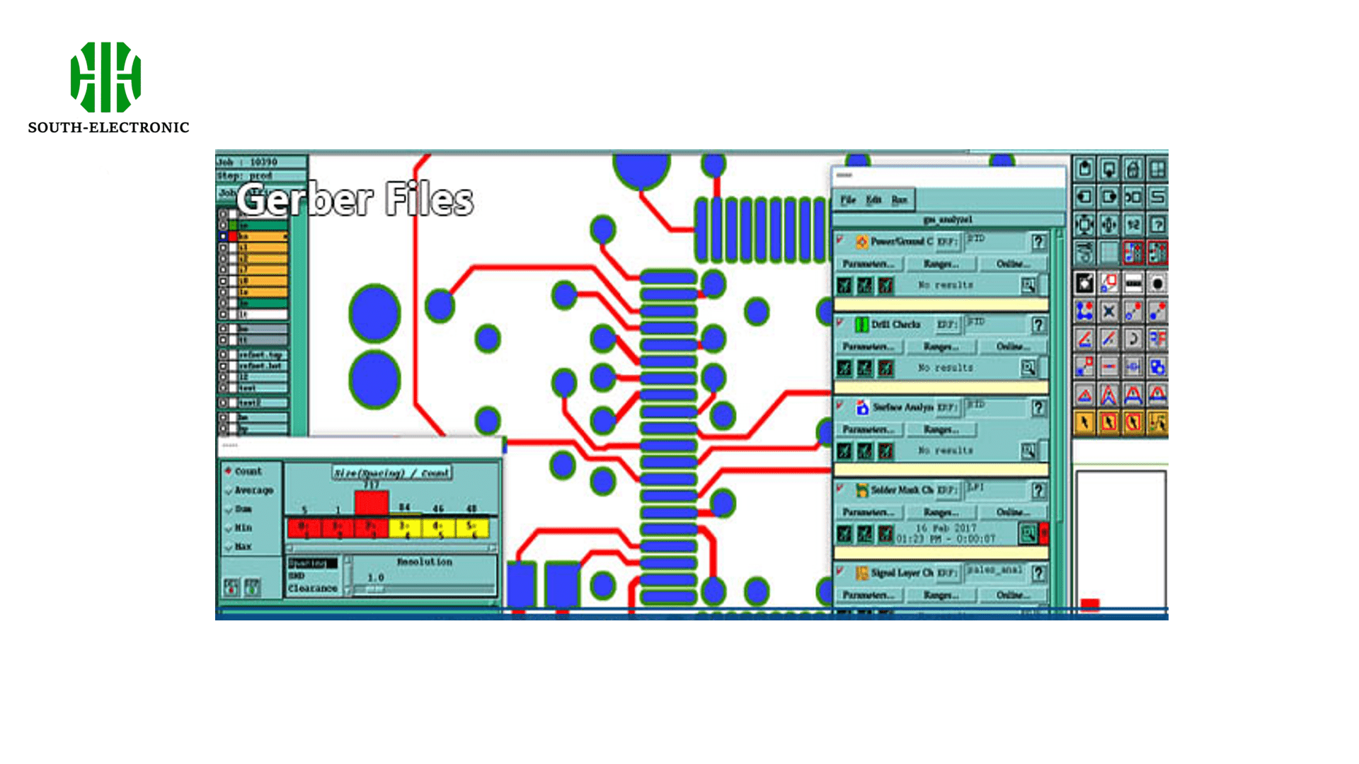
Gerber format is an open 2D binary vector image format for PCB designs. The files of all physical layers are in Gerber format, and we call any of them as Gerber file, and all of them as Gerber files. When verifying PCB Gerber files, it is essential to check that all layers are correctly identified and ordered, verify the accuracy of drill charts and PCB dimensions, ensure that all aperture definitions are correct, and review spacing, trace widths, and clearances. Additionally, using a Gerber viewer to cross-check the design against the schematic is highly recommended.
What Information Do Gerber Files Contain?
1. Layer Information:
- Copper Layers: Top and bottom copper layers, including inner layers for multi-layer boards.
- Solder Mask Layers: Defines the areas where solder mask should be applied.
- Silkscreen Layers: Contains the component labels and other markings on the board.
2. Drill Information:
- Drill Charts: Specifies the location and size of all holes, including vias and mounting holes.
3. Aperture Definitions:
- Aperture List: Defines the shapes and sizes of the tools used to create pads and traces.
4. Board Outline:
- Outline Layer: Defines the physical shape and size of the PCB.
5. Dimensions and Specifications:
- Dimension Details: Accurate measurements for manufacturing the PCB.

How to Verify Gerber Files?
| Verification Step | Description |
|---|---|
| Use a Gerber Viewer | Load and visually inspect each layer of the PCB design. |
| Cross-Check Against the Schematic | Print to 1:1 scale, place components on printout to verify footprints. |
| Verify Layer Order and Identification | Ensure all layers are present, identified, and ordered correctly. |
| Check Aperture Definitions | Review the aperture list for accuracy and consistency. |
| Inspect Drill Charts and PCB Dimensions | Compare with design specifications to ensure accuracy. |
Recommended Tools for Verifying Gerber Files
| Tool | Description |
|---|---|
| Gerbv | Free, open-source Gerber viewer. |
| ViewMate | Advanced Gerber viewer with inspection features. |
| Altium Designer | Comprehensive PCB design and verification tool. |
How to Read a Gerber File?
Reading a Gerber file involves understanding the commands and data that define the PCB layout.
1. Load the File in a Gerber Viewer:
- Use tools like Gerbv or ViewMate to open the Gerber file.
2. Identify Key Elements
- Look for key elements such as copper traces, pads, and drill holes.
3. Cross-Reference with Design Specifications
- Ensure that all elements match the design specifications and requirements.
4. Verify Measurements
- Check measurements and dimensions to ensure they are accurate and consistent with the design.
Making sure your PCB Gerber files are accurate is super important when you’re getting ready to manufacture your boards. You want to make sure everything is right before you send it off to the fab house. You don’t want to pay for a bunch of boards that have a mistake on them. You don’t want to have to do a respin because you forgot to include a drill file or something like that. You want to make sure everything is right before you send it off. You want to make sure all the layers are in the right order, that all the apertures are defined correctly, and that everything is going to be perfect. You want to make sure you’re using the right tools and following best practices to make sure everything is going to be perfect.

