
Custom HDI PCB Manufacturing Services
Min trace 3/3 mil | ENIG / HASL | FR-4 & High-TG | AOI & E-Test
We manufacture high-precision HDI PCBs for telecommunications, consumer electronics, and advanced industrial applications, ensuring stable quality and consistent performance for repeat production.
HDI PCB Capabilities
HDI PCB Process Capability
-
Layer Count
up to 68 layers
-
PCB Dimensions
≤24*48inch(610*1220mm)
-
Materials Types
FR-4 | High Tg | Halogen-free | PTFE | Ceramic PCB | Metal substrate material
-
Material Brand
Lianmao|Shengyi| Taiyao| Nanya, Panasonic|Isola|Nelco|Rogers|Taconic|Arlon...
-
Board Thickness
0.2mm-8.0mm
-
Finish Treatment
Immersion Gold|Lead-free HASL|OSP|Immersion Tin|Immersion Silver|Thick Gold Plating|Silver Plating|Immersion Gold+OSP
-
Copper thickness
0.33 OZ-8 OZ
-
SolderMask Color
Green| Blue| Black|Yellow| Red|Purple| White...
-
Finish Treatment
Immersion Gold|Lead-free HASL|OSP|Immersion Tin|Immersion Silver|Thick Gold Plating|Silver Plating|Immersion Gold+OSP
Why Choose Us for HDI PCB Manufacturing
We support engineers with reliable HDI PCB manufacturing,
from prototype builds to stable repeat production.
Every HDI PCB is meticulously reviewed by our engineers to ensure optimal stack-up, impedance control, and manufacturability before production.
We prioritize consistent quality across all batches, catering to both prototypes and long-term production needs.
Experienced in tight trace/space, controlled impedance, and multilayer lamination for intricate HDI designs.
We provide clear technical communication and fast responses to effectively support overseas engineering and purchasing teams.
Related Project We Had Done
HDI PCB for Telecommunications Equipment
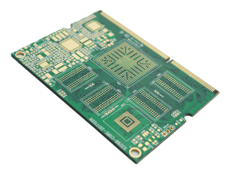
Application
Key Specs
Challenge
Result
HDI PCB for Medical Devices
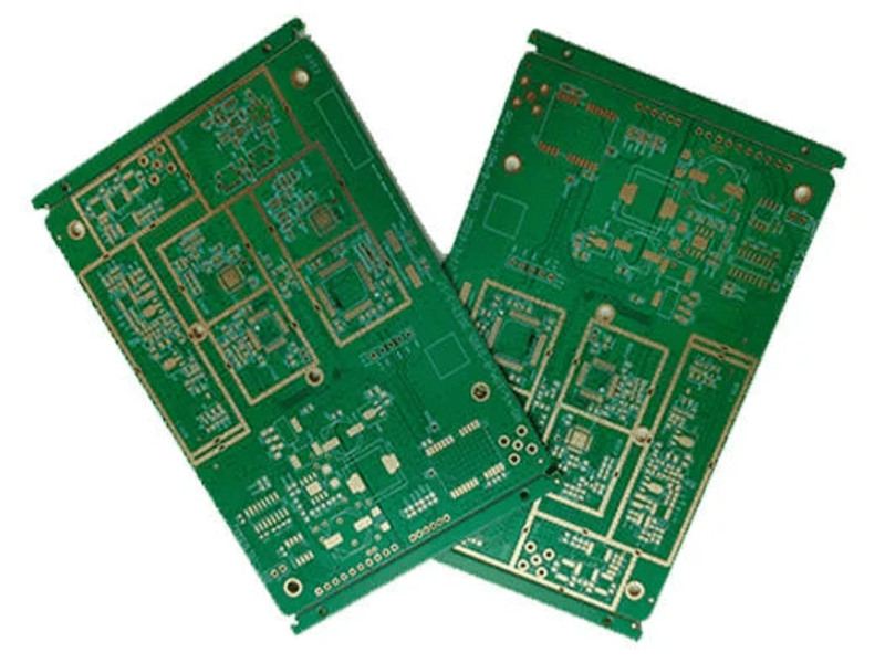
Application
Key Specs
Challenge
Result
HDI PCB for Consumer Electronics
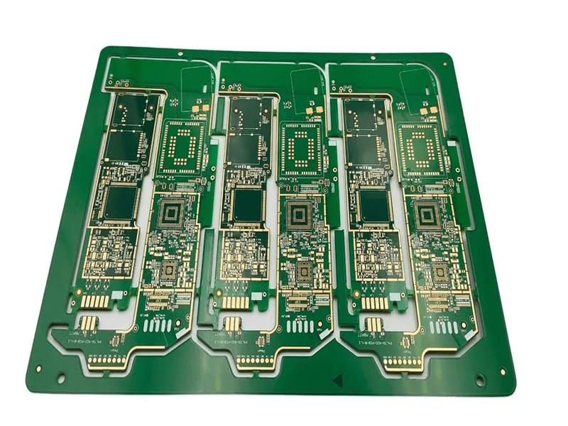
Application
Key Specs
Challenge
Result
Quality Control & Certifications for HDI PCB Production
Common Questions
Most Popular Questions
What is the typical lead time for HDI PCB production?
Prototype lead time is typically 7–10 working days.
Mass production lead time depends on quantity and specifications.
What is the minimum order quantity for HDI PCBs?
How do you handle shipping for HDI PCB orders?
Can you provide engineering support for my HDI PCB design?
What files are required to get an HDI PCB quotation?
Please provide Gerber files, PCB quantity, and any special requirements such as impedance control or material preference.
Send Us a Message
The more detailed you fill out, the faster we can move to the next step.

