

Modern gadgets keep shrinking while demanding more power – can traditional circuit boards keep up? Multilayer PCBs emerged as the silent hero powering your smartphone’s brain surgery-level precision in a pocket-sized device.
A multilayer PCB[^1] stacks 4-60 conductive copper layers[^2] with insulating dielectric materials, enabling complex circuitry in minimal space. These boards solve modern electronics’ core dilemma: packing more functionality into shrinking devices without compromising speed or reliability.
While we marvel at sleek devices, the real magic happens in their hidden skeletal systems. Let’s dissect what makes multilayer PCBs the foundation of today’s tech revolution.
The Anatomy of a Multilayer PCB: What’s Inside?
Your smartphone contains more engineering than Apollo 11’s guidance computer – and it all starts with these layer cake-like boards. Imagine 12 ultra-thin circuit layers working in perfect sync, each with specialized roles.
A typical multilayer PCB contains alternating conductive copper layers (signal, power, ground) and dielectric insulation[^3], bonded under high heat/pressure. Critical components include prepreg adhesive sheets, copper foil, solder mask, and silkscreen markings for component placement.
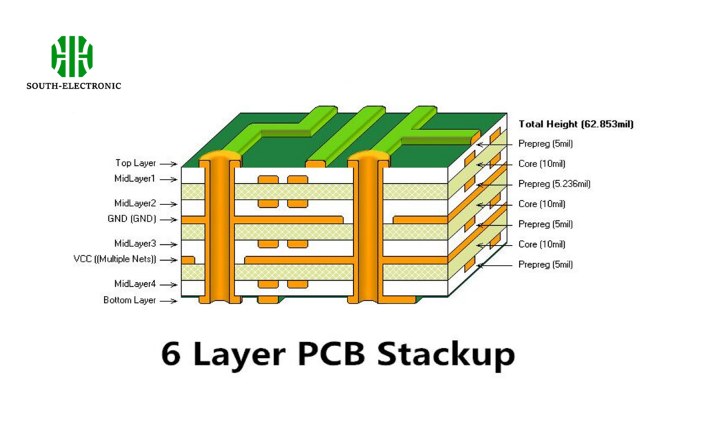)
Layer Hierarchy and Functions
| Layer Type | Thickness Range | Primary Function | Common Materials |
|---|---|---|---|
| Signal Layers | 0.5-3 oz Cu | Transmit electronic signals | Electrolytic copper foil |
| Power Plane | 2-4 oz Cu | Distribute stable voltage | Rolled annealed copper |
| Ground Plane | 2-4 oz Cu | Provide electrical reference/EMI shield | Low-profile copper |
| Dielectric Layers | 0.1-0.3mm | Insulate conductive layers | FR-4, Polyimide, Rogers |
| Solder Mask | 0.01-0.03mm | Prevent accidental short circuits | Liquid photoimageable ink |
The real engineering feat lies in the layer stackup sequence. High-speed designs alternate signal layers with ground planes to control impedance, while power-hungry devices need dedicated voltage layers. Modern 16-layer boards can contain 6 signal layers, 4 ground planes, 3 power planes, and 3 specialized layers for high-frequency signals.
Why Choose Multilayer Over Single-Layer?
Would you build a skyscraper with only floor plans? Single-layer boards work for simple calculators, but modern devices need 3D circuit architecture. Consider Apple’s M1 chip – its 16-core brain requires 12-layer boards for signal routing.
Multilayer PCBs enable 10x higher component density vs single-layer, reduce EMI[^4] by 60-80% through dedicated ground planes, and improve signal speed by 30% via controlled impedance routing[^5]. They allow complex power distribution impossible in single-layer designs.
)
Performance Benchmark Table
| Parameter | Single-Layer | 4-Layer PCB | 8-Layer PCB |
|---|---|---|---|
| Max Frequency | 500 MHz | 2 GHz | 6 GHz |
| EMI Radiation | High | Moderate | Low |
| Power Stability | ±15% | ±5% | ±1% |
| Repair Difficulty | Easy | Moderate | Complex |
| Typical Cost | $0.50 | $2.50 | $6.80 |
| Design Time | 2 Days | 1 Week | 3 Weeks |
While costs increase initially, multilayer boards save money long-term through reliability. Medical devices using 8-layer boards show 99.992% uptime vs 97.4% for single-layer equivalents. Automotive ECUs require multilayer designs to handle -40°C to 150°C operational ranges that would crack simpler boards.
Key Materials Used in Multilayer Boards
Not all PCBs are created equal – material choice determines whether your device survives a drop or melts under load. The wrong dielectric can turn your gadget into a paperweight.
Critical materials include FR-4 epoxy[^6] (70% market share) for standard boards, polyimide for flexible circuits, and ceramic-filled PTFE for 5G/mmWave. Copper purity (99.7%+), glass transition temperature (Tg), and dielectric constant (Dk) are decisive quality factors.
)
Material Comparison Matrix
| Material | Tg (°C) | Dk @1GHz | Cost Factor | Best For |
|---|---|---|---|---|
| FR-4 Standard | 130-140 | 4.5 | 1x | Consumer electronics |
| High Tg FR-4 | 170-180 | 4.3 | 1.8x | Automotive/Power systems |
| Polyimide | 250+ | 3.5 | 3x | Flexible/Aerospace |
| Rogers 4350B | 280 | 3.48 | 12x | 5G/RF circuits |
| Aluminum Base | 150 | 4.5 | 2.5x | LED lighting/Power modules |
Material selection directly impacts performance. While Rogers materials[^7] enable 77GHz automotive radars, their $12/sq.ft cost justifies only military/aerospace use. Most smartphones use modified FR-4 with halogen-free flame retardants (ROHS compliant) and 105µm copper foil for 5G antennae.
Common Misconceptions About Multilayer PCBs
"More layers always mean better performance" – that’s like saying taller buildings are always better. Design quality trumps layer count, and improper stackups can ruin even 16-layer boards.
Myth 1: "Multilayer PCBs are too fragile". Reality: Proper via protection and material selection enable military-grade durability. Modern HDI boards[^8] withstand 5000+ thermal cycles.
)
Myth vs Fact Analysis
| Misconception | Engineering Reality |
|---|---|
| "Thicker boards last longer" | Thinner 0.8mm 8-layer often outlast 1.6mm 2-layer due to better heat dissipation |
| "Slow signals need fewer layers" | Even 1MHz power systems benefit from separate ground planes reducing noise |
| "Blind vias reduce reliability" | Laser-drilled microvias (50µm) in smartphones show >97% yield rates |
| "More layers = higher EMI" | Proper layer sequencing cuts EMI by 18dB vs unoptimized stackups |
A classic example is automotive ADAS systems: 6-layer boards with 18µm copper achieve better crash survivability than thicker 4-layer alternatives. The key lies in simulation-driven designs, not just layer count.
Conclusion
Multilayer PCBs enable technology’s shrinking yet smarter evolution – these microscopic skyscrapers prove that in electronics, depth beats surface area every time.
[^1]: Explore the advantages of multilayer PCBs, which are crucial for compact and efficient electronic devices, enhancing performance and reliability.
[^2]: Understanding the role of conductive copper layers can deepen your knowledge of PCB design and its impact on device performance.
[^3]: Learn about dielectric insulation’s role in preventing electrical interference, essential for the reliability of modern electronics.
[^4]: Discover various strategies to minimize EMI, ensuring better performance and reliability in electronic devices.
[^5]: Learn how controlled impedance routing enhances signal speed and reduces interference, crucial for high-speed designs.
[^6]: Learn about FR-4 epoxy, the most widely used material in PCBs, and its significance in ensuring device durability and performance.
[^7]: Explore the advantages of Rogers materials for high-frequency applications and their role in advanced PCB designs.
[^8]: Learn about HDI boards and how they contribute to durability and performance in complex electronic systems.

