
مقدمة
في عالم التكنولوجيا سريع التطور، تقف الوحدات الضوئية لثنائي الفينيل متعدد الكلور في المقدمة، مما يحدث ثورة في أنظمة نقل البيانات والاتصالات. قد تبدو الوحدة الضوئية بسيطة، ولكنها في الواقع تخضع لعملية إنتاج طويلة إلى حد كبير. تشتمل مكونات الوحدة الضوئية على الأجهزة البصرية والغلاف ولوحة PCB.
تطبيق منتجات الوحدة البصرية
المتطلبات الفنية لمنتجات الوحدات الضوئية صارمة، نظرًا لوظيفتها الحيوية في نقل البيانات. تتضمن الميزات الأساسية القدرة على نقل الإشارات بسرعة عالية، والحد الأدنى من استهلاك الطاقة، وتقليل فقدان الإشارة. ومن المتوقع أيضًا أن تكون هذه الوحدات مدمجة ومتينة ومتعددة الاستخدامات وقادرة على العمل في ظل مجموعة من الظروف البيئية. علاوة على ذلك، يعد التوافق مع الأنظمة الأساسية والمعايير المختلفة أمرًا ضروريًا، مما يضمن التكامل السلس في بنيات الشبكات المختلفة.
المتطلبات الفنية لمنتجات الوحدات الضوئية
يتم تحديد الدور المحوري لمنتجات الوحدات الضوئية في اتصالات البيانات بشكل أساسي من خلال: (1) تعبئة الوحدة الضوئية؛ (2) سرعة نقل الوحدة الضوئية؛ (3) متطلبات التطبيق المحددة للوحدة البصرية، مثل التبريد، ومقاومة التوصيل الساخن، والاستخدام في البيئات الصناعية المختلفة. يعد التوافق مع الأنظمة الأساسية والمعايير المتعددة عاملاً أساسيًا آخر، مما يضمن التكامل السلس في بنيات الشبكات المختلفة.
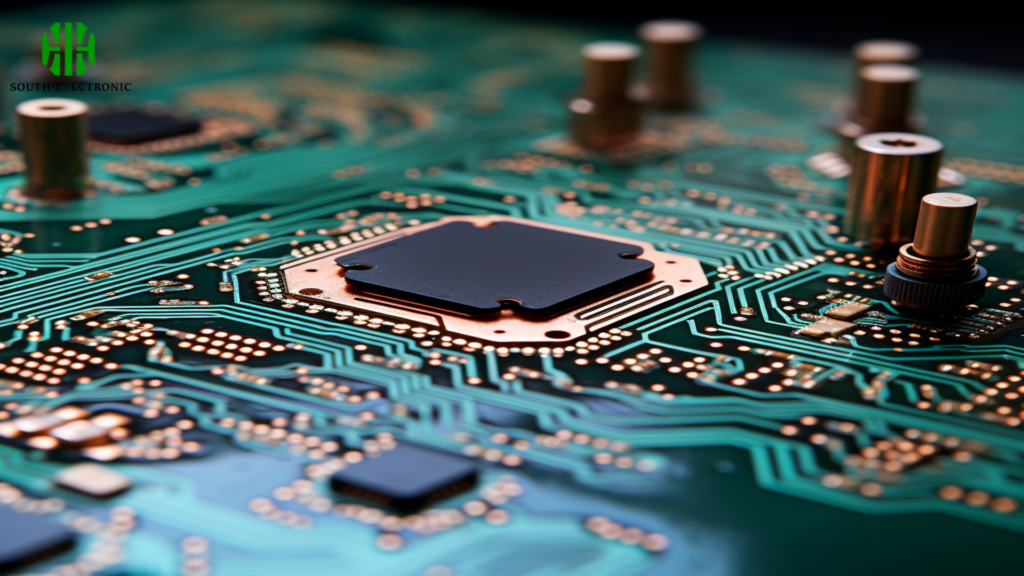
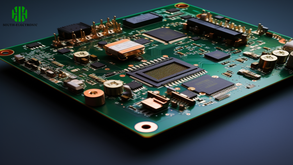
الخصائص التقنية للوحدة الضوئية PCB
إن الخصائص التقنية لمركبات ثنائي الفينيل متعدد الكلور في الوحدات الضوئية هي ما يميزها. تم تصميم مركبات ثنائي الفينيل متعدد الكلور هذه للتعامل مع عمليات إرسال الإشارات عالية السرعة، مما يتطلب تحكمًا دقيقًا في المعاوقة والحد الأدنى من تداخل الإشارة. غالبًا ما يتم استخدام المواد المتقدمة مثل الشرائح عالية التردد لتلبية هذه الاحتياجات. بالإضافة إلى ذلك، تعد الإدارة الحرارية جانبًا بالغ الأهمية، حيث يجب على مركبات ثنائي الفينيل متعدد الكلور أن تبدد الحرارة بشكل فعال للحفاظ على استقرار الأداء. يتم حساب تصميم طبقة المكدس وسمك النحاس وعرض التتبع بدقة لضمان الأداء الأمثل.
التحكم في العمليات الرئيسية للوحدة الضوئية PCB
يعد التحكم الرئيسي في العمليات في تصنيع الوحدات الضوئية لثنائي الفينيل متعدد الكلور أمرًا حيويًا للحفاظ على الجودة والموثوقية. يتضمن ذلك فحوصات صارمة للجودة في كل مرحلة، بدءًا من التصميم وحتى التجميع. يتم استخدام تقنيات مثل الفحص البصري الآلي (AOI) والفحص بالأشعة السينية للكشف عن أي عيوب. يعد ضمان دقة تطبيق معجون اللحام، ووضع المكونات، وعمليات اللحام بإعادة التدفق أمرًا بالغ الأهمية أيضًا. علاوة على ذلك، يتم إجراء الاختبارات البيئية، بما في ذلك اختبارات مقاومة درجة الحرارة والرطوبة، لضمان الموثوقية على المدى الطويل.
خاتمة
تعتبر الوحدات الضوئية لثنائي الفينيل متعدد الكلور محورية في قيادة الجيل القادم من تقنيات اتصالات البيانات. تطبيقاتها واسعة، والمتطلبات الفنية صارمة، وتتطلب الدقة في كل من عمليات التصميم والتصنيع. يعد فهم الخصائص التقنية والحفاظ على التحكم الصارم في العملية أمرًا ضروريًا لتطوير منتجات الوحدات الضوئية الموثوقة والفعالة. مع استمرار تقدم التكنولوجيا، لا يمكن المبالغة في تقدير دور الوحدات الضوئية لثنائي الفينيل متعدد الكلور في تشكيل مستقبل نقل البيانات والاتصالات. وسيكون تطورها عاملاً رئيسياً في السعي المستمر لتحقيق اتصال رقمي أسرع وأكثر كفاءة وموثوقية، مما يمثل حقبة مثيرة في عالم الاتصالات وما بعده.


