
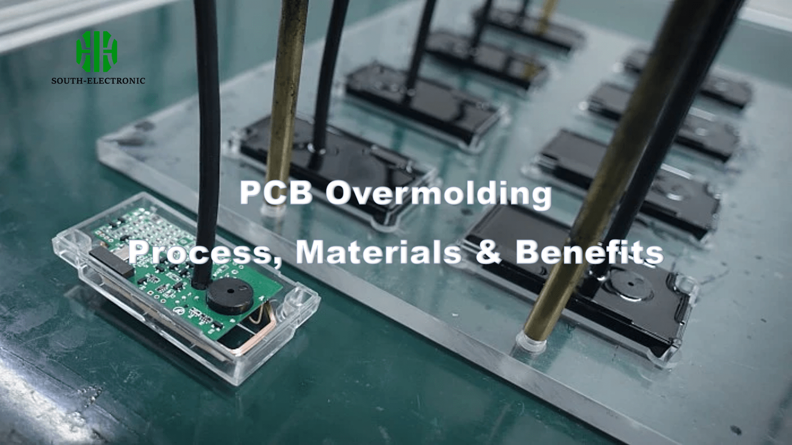
Your circuit boards are vulnerable. Moisture creeps, vibrations shake connections, and thermal shifts crack solder joints. PCB overmolding eliminates these failure points through precision encapsulation. Let’s explore why this process dominates harsh-environment applications today.
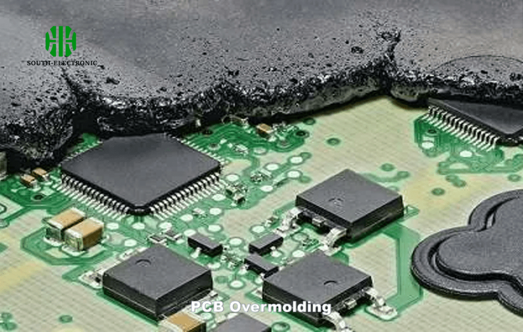
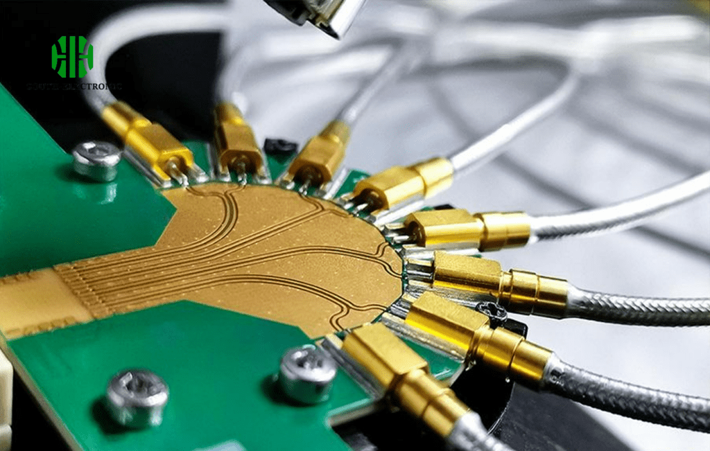
PCB overmolding[^1] injects molten polymer around assembled electronics, forming a seamless protective layer. This process shields components from water, dust, chemicals, and mechanical stress while offering custom geometries – achieving IP68 protection[^2] at 60% lower weight than metal enclosures.
While the concept seems straightforward, successful implementation demands expertise. I once saw a $20k medical sensor fail because the designer chose the wrong shore hardness. Let’s dissect critical considerations across four domains.
What Exactly Happens During the PCB Overmolding Process?
Picture injecting hot plastic over fragile components without damaging them. Overmolding requires surgical precision – here’s how technicians achieve it.
The process starts with PCB preheating (80-120°C) to prevent thermal shock[^3]. Injection-molded thermoplastics or liquid silicone then flow at 150-300°C, controlled within ±2°C tolerance. Molds clamp at 50-100 tons pressure for <0.1mm material variance.
Critical Process Breakdown
| Stage | Parameters | Failure Risks |
|---|---|---|
| Preheating | 80-120°C for 15-30 mins | Delamination if uneven heating |
| Injection | 150-300°C @ 500-1500 psi | Burnt components exceeding Tg |
| Curing | 60-180 sec dwell time | Voids with premature ejection |
| Demolding | <1% mold deflection | Cracked edges if adhesion mismatch |
In automotive applications, I use IR preheaters achieving ±5°C uniformity – anything less causes resin pooling. The injection phase demands material-specific flow rates: silicones need 50-100 mm/sec versus 200-300 mm/sec for TPU. Post-curing reduces residual stress by 40% through controlled cooldown ramps.
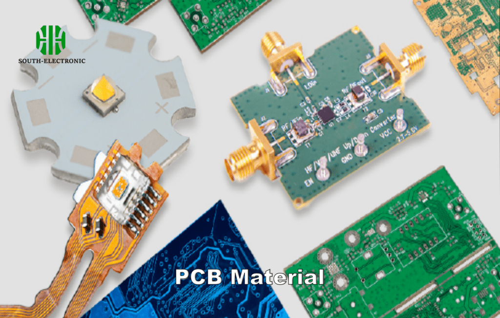
Which Overmolding Material Best Suits Your Application?
Choose wrong, and your underwater drone's housing will crack at 30m depth. Material selection separates reliable products from field failures.
Liquid silicone rubber (LSR)[^4] excels in -50°C to 200°C ranges with 500% elongation. Thermoplastic polyurethane (TPU)[^5] offers better abrasion resistance (80 Shore A) but degrades above 120°C. For EMI shielding, carbon-filled PBT composites reduce interference by 25dB.
Material Performance Matrix
| Property | LSR | TPU | Epoxy |
|---|---|---|---|
| Temp Range | -50°C~200°C | -40°C~120°C | -20°C~150°C |
| Cycle Life | 1M+ flexes | 500k flexes | Brittle after 10k |
| Chemical Resistance | 10/10 acids | 7/10 oils | 9/10 solvents |
| Tooling Cost | $80k+ | $25k | $15k |
Medical IoT devices demand USP Class VI LSR that withstands autoclaving. I specify 30-50 Shore hardness for wearables to prevent skin irritation. High-voltage gear requires UL94 V-0 flammability-rated materials – a client saved $420k/year switching from potting to flame-retardant TPU.
How Does Overmolding Reduce Total Production Costs?
Upfront molding costs scare many – until they see the 5-year TCO. Overmolded boards slash four hidden expenses.
Eliminating secondary enclosures cuts assembly labor by 65%. Automated molding lines achieve 98% yield versus 85% for manual potting. Reduced part count decreases warranty claims by 40% through improved reliability.
Cost Reduction Drivers
| Factor | Traditional Assembly | Overmolded |
|---|---|---|
| Parts Count | 12-18 components | 1 molded piece |
| Assembly Time | 22 minutes/unit | 8 minutes/unit |
| Testing Cost | $4.50/unit (IP67 test) | $0.50/unit (in-mold QA) |
| Rework Rate | 15% | 3% |
A drone manufacturer reduced BOM from 19 parts to 3 using overmolding, cutting assembly labor from $8.20 to $2.75 per unit. In-mold laser marking saved $0.18/unit versus silk-screening. The sealed design eliminated $12k/year in salt spray testing.
What Design Errors Destroy Overmolded PCB Reliability?
I’ve seen 2mm standoffs sink entire batches. These four design flaws turn robust boards into ticking time bombs.
Inadequate thermal relief pads[^6] cause delamination under 50°C swings. Undersized keep-out zones[^7] (less than 1.5mm) lead to flash leakage. Wrong draft angles[^8] (under 3°) rip circuits during demolding. Component height variance over 0.3mm creates stress points.
Failure Avoidance Checklist
| Flaw | Acceptable Range | Failure Mode |
|---|---|---|
| Standoff Height | 0.5-2.0mm | Solder cracks if >2.5mm |
| Bond Line Thickness | 2-4mm | Cracks if <1.5mm |
| Venting Channels | 0.8mm² vent/cm³ | Voids without pressure equalization |
| Insert Material CTE | <15 ppm/°C | Cracked joints if CTE mismatch over 8 ppm |
For automotive ECUs, I specify 2.5mm minimum encapsulation over high-current traces. One client learned the hard way – 0° draft angles on connectors caused 22% scrap from torn pads. Always include 1% mold shrinkage allowance in cavity dimensions.
Conclusion
PCB overmolding cuts lifecycle costs by 40% through integrated protection. By mastering material selection, process controls, and DFM principles, engineers achieve IP69K reliability without bulky enclosures – the future of rugged electronics.
[^1]: Understanding PCB overmolding is crucial for anyone involved in electronics design, as it enhances durability and performance in harsh environments.
[^2]: Exploring IP68 protection will help you grasp how it safeguards electronics from water and dust, ensuring longevity and reliability.
[^3]: Learning about thermal shock can prevent costly failures in electronic devices, making it essential for designers and engineers.
[^4]: Explore the advantages of LSR, including its temperature range and flexibility, crucial for applications like underwater drones.
[^5]: Learn about TPU’s abrasion resistance and its applications, especially in high-performance environments.
[^6]: Understanding thermal relief pads is crucial for preventing delamination and ensuring PCB reliability. Explore this link for in-depth insights.
[^7]: Keep-out zones are vital for preventing flash leakage. Learn more about their importance in PCB design by checking this resource.
[^8]: Draft angles play a critical role in preventing circuit damage during demolding. Discover more about their impact on PCB reliability here.


