

Imagine wasting 30% of production materials because your PCB boards warp during assembly. Worse yet, broken components delay deliveries as half your batch fails quality checks. That’s why panelization exists.
PCB panelization[^1] combines multiple circuit boards into a manufacturing unit, optimizing automated production while preventing material warping and component damage. It reduces scrap rates by maintaining dimensional stability[^2] during SMT processes and adheres to IPC standards for precision fabrication.
)
Now that we understand the basics, let’s explore how to implement panelization effectively across different PCB types – including delicate flexible circuits that demand specialized handling.
PCB Panel Design Tips: How to Avoid Common Mistakes?
You’ve finalized your circuit design, but automated assembly machines keep rejecting the panels. Why? Suboptimal panelization sabotaged your layout.
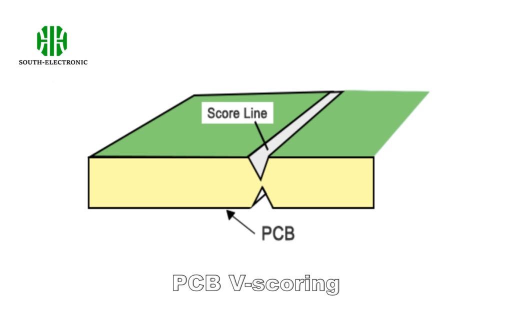
Effective PCB panelization requires calculating optimal breakaway tab spacing (5-8mm), V-scoring depth[^3] (1/3 board thickness), and directional routing to minimize stress points. Always align component placement with depaneling machine pathways to prevent collision during separation.
)
Three Critical Design Rules for High-Yield Panels
-
Tab Placement Strategy Tab Type Usage Scenario Breakaway Force Solid Tab Heavy components 15-20N Perforated Tab Standard boards 8-12N No Tab Laser depaneling N/A -
Material Expansion Margins
Add 0.5mm spacing between adjacent boards in high-temperature applications to accommodate thermal expansion[^4] – especially crucial for ceramic-filled PTFE substrates. -
Fiducial Alignment
Place three global fiducials (1mm diameter) forming a triangular pattern, minimum 5mm from panel edges. This enables robotic systems to compensate for ±0.2mm positional drift.
How to Reduce PCB Scrap Rate Through Panelization?
Your 8-layer HDI board scrap rate jumped to 18% last quarter. Could optimal panelization have saved $47,000 in materials?
Panelization reduces PCB scrap by 22-35% through efficient material utilization and automated handling compatibility. The key is maximizing board count per panel while maintaining depaneling reliability – typically achieving ≥92% first-pass yield when following IPC-7351A standards[^5].
)
Scrap Reduction Techniques by Board Type
| Board Type | Optimal Panel Size | Breakaway Method | Scrap Rate Benchmark |
|---|---|---|---|
| Rigid FR-4 | 18"×24" | V-cut | ≤5% |
| Aluminum | 12"×18" | Punching | 7-9% |
| Flex-Rigid | 8"×12" | Laser | 3-4% |
For lead-free HASL boards, implement these steps:
- Calculate gold finger overlap (minimum 0.8mm)
- Use mouse bites with 0.55mm holes spaced at 1.2mm intervals
- Apply 45° scoring for multilayer separation
What Are the Special Requirements for Flexible Circuit Board Panelization?
That flexible ECG sensor failed after 800 bend cycles? Improper panelization likely caused cumulative stress damage.
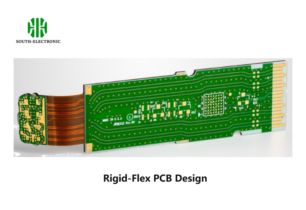
Flexible PCB panelization[^6] requires polyimide stiffener placement[^7], curved V-grooves following bend radii (≥3x board thickness), and tension-controlled depaneling tools[^8]. Critical parameters include 0.1-0.15mm coverlay overlap and ≥1.5mm spacing from active circuits to panel edges.
Flexible Panel Design Matrix
| Parameter | Static Flex | Dynamic Flex | Rigid-Flex |
|---|---|---|---|
| Bend Radius | 10× thickness | 100× cycles | 6X thickness |
| Stiffener Thickness | 0.2mm | 0.1mm | 1.6mm |
| Routing Offset | 0.3mm | 0.5mm | 0.2mm |
Implementation checklist:
- Use diamond-coated router bits (Ø1.0-1.6mm) for clean cuts
- Maintain 88°±2° blade angle during depaneling
- Apply PSA masking on contact pads before routing
Conclusion
Strategic PCB panelization balances production efficiency with reliability, reducing scrap rates by 20-35% through optimized layouts and breakaway techniques while ensuring assembly compatibility – critical for modern high-density electronics manufacturing.
[^1]: Understanding PCB panelization can significantly enhance your production efficiency and reduce waste. Explore this resource to learn more.
[^2]: Dimensional stability is crucial for maintaining quality in PCB production. Discover its significance and how to achieve it effectively.
[^3]: Knowing the right V-scoring depth can prevent damage during assembly. This link will provide insights into best practices for your PCB designs.
[^4]: Understanding thermal expansion is crucial for designing reliable PCBs, especially in high-temperature applications. This link will enhance your knowledge on the topic.
[^5]: Learning about IPC-7351A standards will help you achieve higher yields and better quality in PCB manufacturing, making it a valuable resource.
[^6]: Explore this resource to understand the essential techniques and considerations for effective Flexible PCB panelization, ensuring reliability and efficiency.
[^7]: Learn about the significance of polyimide stiffener placement in PCB design to enhance durability and performance in flexible circuits.
[^8]: Discover how tension-controlled depaneling tools can improve the quality and precision of PCB manufacturing processes.

